Tag Archives: FPGA


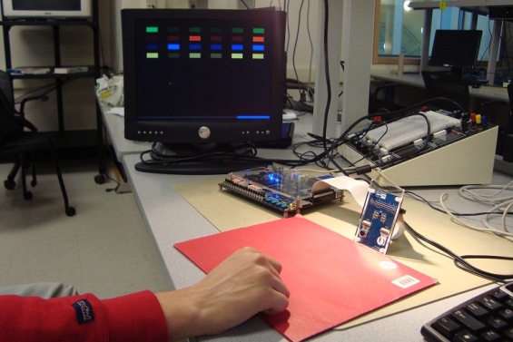
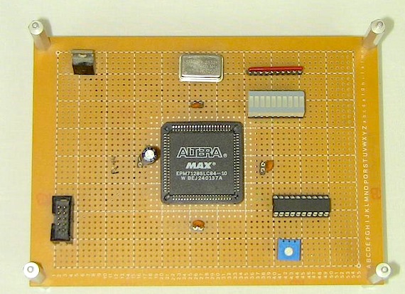
Breakout board for DE0-Nano FPGA development board

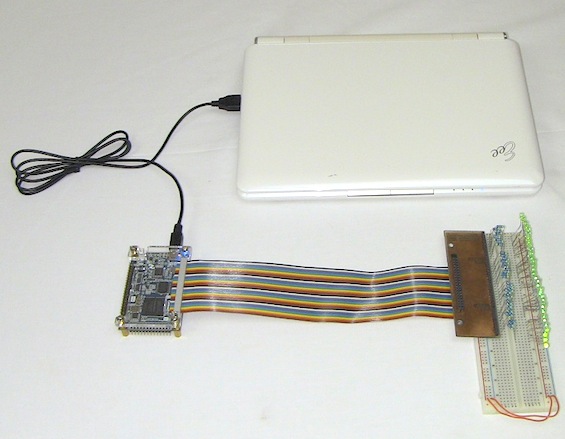
DE0-Nano is a great FPGA development and education board featuring the Altera Cyclone® IV 4C22 FPGA with 22,320 Logic elements (LEs), 594 Embedded memory (Kbits), 66 Embedded 18 x 18 multipliers, 4 General-purpose PLLs, and 153 Maximum FPGA I/O pins. Since not all of these I/O pins are used very often, Chris from PyroElectro has made his own expansion board for easy prototyping with DE0-Nano.

Breakout board for DE0-Nano

He designed a PCB for his breakout board that basically connects to the 2×20 pin headers on the DE0-Nano through an IDE cable and makes those I/O pins easily available for prototyping on breadboard.

Play the classic Breakout game with hand motions

A group of students at Cornell university designed a new version of the classic Breakout game. The traditional way of playing the game is through key presses that moves the paddle left and right in order to bounce the traveling ball upward, keeping it in play. However, in this new design the player can move his hand left, right, up, or down to control the paddle accordingly. A CCD camera was used to sense the motion of the hand. The image captured by the camera was processed by the Altera® DE2 FPGA Development board to detect the hand position in the image frame. The game is displayed on a VGA monitor.

Breakout game played with motion of a hand

Watch this project in action.

Interfacing an external ADC chip to FPGA/CPLD

Chris (from PyroElectro) has posted an article on interfacing an external ADC chip to FPGAs and CPLDs, which do not have A/D capabilities built-in. He illustrates the idea with an Altera EPM7128 and a MAX150 8-bit analog to digital converter IC. The test analog signal is derived using a potentiometer and the converted digital output is shown using an LED bargraph display. The interface between the CPLD and ADC has been implemented in VHDL.

Interfacing an ADC to CPLD