Expanding the number of I/O lines using Microchip MCP23008
|
|
A microcontroller comes with a limited number of general purpose input and output (GPIO) ports. However, some applications may require more ports than are available on the microcontroller. In such a case, GPIO expanders can be used to increase the I/O capability of the microcontroller. MCP23008 is one such device (manufactured by Microchip Technology) which provides an easy I/O expansion using 2-wire serial interface. This tutorial illustrates how to add an extra 8-bit I/O port to PIC12683 microcontroller (which has only 6 I/O pins) using MCP23008. A seven segment LED display and a tact switch will be connected to the extended port. The PIC12F683 microcontroller will count the switch presses and display the counter value on the seven segment LED module.

MCP23008 port expander interfaced to PIC12F683
Theory
The MCP23008 an I2C slave device that provides 8-bit, general purpose, bi-directional I/O expansion for I2C bus. If you are not familiarized with I2C protocol, read my article on Inter-Integrated Circuit communication. MCP23008 supports 7-bit slave addressing, with the read/write bit filling out the control byte. The four most significant bits of the slave address are fixed (0100 for MCP23008) and the remaining three bits are user-defined hardware address bits (pins A2, A1 and A0). This allows us to connect up to eight MCP23008 devices on a common I2C bus. The control byte format for MCP23008 is shown below.

I2C control byte format for MCP23008
Control and configuration registers
The individual bits of the 8-bit GPIO port can be configured as input or output. The port pins can also be enabled for internal pull up resistor and interrupt-on-change. These operations are controlled through a set of configuration and control registers. The table below shows the list of these registers, their addresses and the power-on reset values.

Configuration and Control registers
These registers are described in the datasheet of MCP23008. I am summarizing them here. We will talk about configuring these registers for our specific purpose in the software section.
I/O Direction (IODIR): It controls the direction of the data I/O. When a bit is set, the corresponding pin becomes an input. When a bit is clear, the corresponding pin becomes an output.
Input Polarity (IPOL): It allows the user to configure the polarity on the corresponding GPIO port bits. If a bit is set, the corresponding GPIO register bit will store the inverted value on the pin.
Interrupt-on-change Control Register (GPINTEN): It controls the interrupt-on- change feature for each pin. If a bit is set, the corresponding pin is enabled for interrupt-on-change. The DEFVAL and INTCON registers must also be configured if any pins are enabled for interrupt-on-change.
Interrupt Control (INTCON): It controls how the associated pin value is compared for the interrupt-on-change feature. If a bit is set, the corresponding I/O pin is compared against the associated bit in the DEFVAL register (described in next paragraph). If a bit value is clear, the corresponding I/O pin is compared against the previous value.
Default Comparison Value (DEFVAL): The default comparison value is configured in the DEFVAL register. If enabled (via GPINTEN and INTCON) to compare against the DEFVAL register, an opposite value on the associated pin will cause an interrupt to occur. For example, if GPINT6 (in GPINTEN), IOC6 (in INTCON) and DEF6 (in DEFVAL) bits are all set, then an interrupt will be generated when the GP6 I/O pin is pulled low. Of course, the GP6 pin direction should be defined as input.
Control Register (IOCON): It contains several bits for configuring the device:
- The Sequential Operation (SEQOP) controls the incrementing function of the address pointer. If the address pointer is disabled, the address pointer does not automatically increment after each byte is clocked during a serial transfer. The power-on-reset value for this bit is 0, which means sequential operation is enabled, and you can send more than 1 byte of data. The address pointer inside MCP23008 will be incremented by 1 after each byte of data clocked in. So if you start writing a byte at 00H register (which is IODIR), the second byte you send will go to IPOL register, third byte will go to GPINTEN, and so on. This is helpful while initializing the MCP23008 where you have to configure the various registers and you can do it by sending the configuration bytes sequentially. But once you are done with the configuration and want to continuously poll (read) or modify (write) a specific register, you can disable the sequential operation by setting SEQOP bit.
- The Slew Rate (DISSLW) bit controls the slew rate function on the SDA pin. If enabled, the SDA slew rate will be controlled when driving from a high to a low.
- The Hardware Address Enable (HAEN) control bit enables/disables the hardware address pins (A1, A0) on the MCP23S08 (SPI version of MCP23008). This bit is not used on the MCP23008. The address pins are always enabled on the MCP23008.
- The Open-Drain (ODR) control bit enables/disables the INT pin for open-drain configuration.
- The Interrupt Polarity (INTPOL) control bit sets the polarity of the INT pin. This bit is functional only when the ODR bit is cleared, configuring the INT pin as active push-pull.
Pull-Up Resister Configuration (GPPU): This register controls the pull-up resistors for the port pins. If a bit is set and the corresponding pin is configured as an input, the corresponding port pin is internally pulled up with a 100 k? resistor.
Interrupt Flag (INTF) Register: It reflects the interrupt condition on the port pins of any pin that is enabled for interrupts via the GPINTEN register. A ‘set’ bit indicates that the associated pin caused the interrupt. This register is ‘read-only’. Writes to this register will be ignored.
Interrupt Capture (INTCAP) Register: It captures the GPIO port value at the time the interrupt occurred. The register is ‘read- only’ and is updated only when an interrupt occurs. The register will remain unchanged until the interrupt is cleared via a read of INTCAP or GPIO.
Port (GPIO) Register: reflects the value on the port. Reading from this register reads the port. Writing to this register modifies the Output Latch (OLAT) register.
Output Latch (OLAT) Register: It provides access to the output latches. A read from this register results in a read of the OLAT and not the port itself. A write to this register modifies the output latches that modify the pins configured as outputs.
Circuit diagram
PIC12F683 does not have hardware I2C module and therefore, the I2C communication with MCP23008 is realized through software using general-purpose I/O pins (GP0 for SCl and GP1 for SDA). A tact switch input is connected to GP7, whereas GP0 through GP6 are defined as outputs and drive a-g segments of a 7-segment LED. The tact switch does not require an external pull-up resistor because internal pull-up is enabled for it. The interrupt output of MCP23008 is read by GP2 pin of PIC12F683.

Circuit Diagram

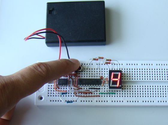
Experimental circuit setup on breadboard
Software
Since PIC12F683 does not have a hardware I2C module, I2C communication is realized using MikroC’s Soft_I2C library routines, which are hardware independent and can be implemented to any GPIO pins. In our experiment, GP0 – GP6 pins of MCP23008 are used as outputs and GP7 as input. The following routine initializes MCP23008 with internal pull-up and interrupt-on-change enabled on GP7. You can see we are using the sequential write operation to configure the registers IODIR through IOCON in sequence. Then the sequential write is disabled and the GPPU register is configured separately after that. The 7-bit slave address for MCP23008 in our circuit is 0100 000. For write operation, the control byte is, therefore, 40H (0100 0000), and for read operation, it is 41H. You can download the complete program for this experiment from the link provided below.
void Init_MCP23008(){
 Delay_ms(10);
 Soft_I2C_Start();     // Issue start signal
 Soft_I2C_Write(0x40); // Slave Address + Write bit
 Soft_I2C_Write(0x00); // Select IODIR register
 Soft_I2C_Write(0x80); // GP0-GP6 O/P, GP7 I/P
 Soft_I2C_Write(0x00); // IPOL
 Soft_I2C_Write(0x80); // GP7 Interrupt-on-change
 Soft_I2C_Write(0x80); // GP7 Def value 1
 Soft_I2C_Write(0x80); // Interrupts on GP7 compares to DEFVAL
 Soft_I2C_Write(0x22); // Disable further sequential write operation
 Soft_I2C_Stop();
// Enable resister pull-up on GP7
 Soft_I2C_Start();     // Issue start signal
 Soft_I2C_Write(0x40); // Address + Write bit
 Soft_I2C_Write(0x06); // Select IODIR register
 Soft_I2C_Write(0x80); // GP7 pull-up
 Soft_I2C_Stop();
}
Download source code and HEX file for this experiment

Counter increments on every button press
References
MCP23008 datasheet from Microchip.
Application note AN1043, Unique Features of the MCP23X08/17 GPIO Expanders, from Microchip.
MCP23X17 is a 16-bit GPIO expander similar to MCP23X08, which is only 8-bit.
|
|
Thanks for sharing such a nice article. I am trying here to run MCP23008 using “”PICkit Serial I2C Demo board”””.. so the GPIO is connected to LEDS. I’m controlling everything with PIC18F2580. The issue here is that I am not getting any output. I ran your code and other codes, used my own. .. but nothing… So, my basic question is , Is it possible to test for I2C on oscilloscope, so the SCL gives a square wave? and if the MCP23008 is fried, will i get a proper clock or it’ll be just high ?
Because I am just getting SDA, SCL high all the time.
Dear,
I’ve already try this basic I2C function and it’s working, i’m still learning about PIC uC world, which code or instruction to modified if i added more I2C device such adding more MCP23008 chip, i’m still confuse about how to selecting which device that i want to control. It would be appreciated if added function with a prompt if device is founded or not.
Pingback: Beaglebone Coding 101: I2C | GigaMegaBlog
Pingback: Decoder for 128 outputs
Pingback: Working with I2C port expanders | You've been blogged!
Pingback: Electronics-Lab.com Blog » Blog Archive » Expand the I/O capability of your microcontroller with MCP23008