Digital logic probe for troubleshooting TTL and CMOS circuits
|
|
A logic probe is considered as a stethoscope for engineers and technicians for debugging digital logic circuits that consists of logic gates, memories, registers, etc. A digital multimeter (DVM) can also be used for such analytical purposes but it gives you the numeric value of the voltage at a point instead of the logic state. Depending on whether the circuit is based on TTL or CMOS components, the voltage levels for logic 0 and 1 could be different for each family. DVM users, thus, have to calculate logic levels from the measured voltages, which consumes time and delays the troubleshooting procedure. A logic probe, on the other hand, does all these functions automatically and shows meaningful logic states at test points. In this project, we will discuss about making a digital logic probe that is applicable to both TTL and CMOS circuits and uses minimal components.

Logic probe for CMOS and TTL circuits
Theory
There are mainly two logic families used in digital circuits: TTL and CMOS. While TTL operates at +5V, the power supply for CMOS circuits could range from +3V to 15V. According to the standard TTL convention, any voltage less than 0.8V is defined as logic low while any voltage above 2.2 is defined as logic high and anything in between these extremes is defined as intermediate state. In case of CMOS circuits, any voltage less than 1/3 of VDD is defined as logic low while any voltage above 2/3 of VDD is defined as logic high. Any voltage between these values is defined as intermediate or transitional state. This logic probe works for both TTL and CMOS circuits powered from +5V to 15V.
This logic probe consists of a 78L05 voltage regulator, a Microchip PIC12F683 microcontroller, a CD4094BE CMOS shift register and a tiny seven segment display. Since the operating voltage range of this logic probe is between 5 to 15V, the role of the 78L05 voltage regulator is to ensure that the microcontroller and the rest of the circuit are always powered with a stable 5V source. There are two voltage divider networks, each made from a 9.1K and a 1K Ohms (1% tolerance) resistors. The outputs of the two networks go to the ADC channels AN0 and AN1. The AN0 channel reads the logic level voltage of the test pin whereas the AN1 channel is used to measure the supply voltage of the test circuit. The information of the supply voltage is necessary to identify a CMOS circuit powered with > 5V. The GP2, GP4, and GP5 pins of PIC12F683 drives the CD4094 shift register. The shift register acts as an I/O expander in this application and its outputs are connected to a seven segment display.

Circuit diagram of the logic probe (click on image to enlarge)
Note: In the above circuit, pins 8 and 16 of CD4094 should be connected to ground and Vcc, respectively.

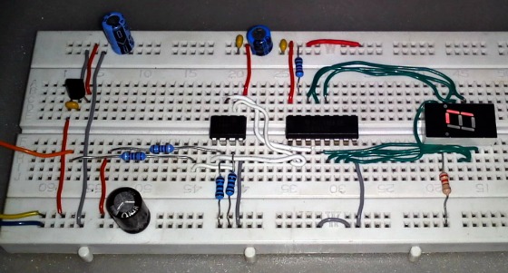
Logic probe circuit setup on a breadboard
Software
The software for this project is written in MikroC PRO for PIC version 5.30. Only the ADC built-in library is used. The rest of the code is written without any library aid. The code starts with the definitions of pin names and common variable declarations. Apart from the main function which does all the tasks, there are six functions in the code. The setup() function sets directions of I/O pins and initiates the built-in ADC for data acquisition. The test_display() function tests the LEDs of the seven segment display connected to the shift register. The way this is done with the shift register will be discussed later in this text. The feature that makes this logic probe universal and unique is its ability to determine the supply voltage level. In the function test_supply(), the power source is tested. During this test if it is found that the ADC average of supply voltage is within the span of 4.75V to 5.25V then the standard TTL minimum high and maximum low logic level voltages are set, otherwise conventional CMOS logic level voltage values are set. These values are kept in the variables called high_level and low_level and are retained till power down. The display(unsigned char val) function is a software-hardware link between the shift register and the micro. It converts any 8 bit value given to the variable val in a way that it can be sent as an output just like a regular I/O port. The strobe pin is at first kept low to allow the access of the internal latches of the CD4094. Eight clock pulses are needed to shift data into the latches. During each clock pulse to the shift register, the variable val’s most significant bit (MSB) is read first and is sent as a data to the data input of the shift register. After sending data to the data pin, val is left shifted once and the clock pin is also toggled once. At the end of eight cycles the strobe pin is pulled high and the display is updated. The adc_avg(unsigned char ch) function read the designated ADC channel by taking 16 samples of ADC data and converting these samples into an average voltage value. Lastly the check_logic() function checks the logic input and sends logic symbol data to the seven segment display.
//Definition of shift register pin names//
#define     data_pin        GP5_bit
#define     clock_pin       GP4_bit
#define     strobe_pin      GP2_bit

//Definition of global variables//
float high_level = 0.0;           //minimum logic high voltage value storage
float low_level = 0.0;            //maximum logic low voltage value storage
const unsigned short disp [4] =
{0x38, 0x3E, 0x76, 0x00};         //Symbols for display - L, U, H and blank

//Function prototypes//
static void setup(void);
static void test_display(void);
static void test_supply(void);
void display(unsigned char val);
float adc_avg(unsigned char ch);
void check_logic(void);

void main(void)
{
    setup();           //Setup the micro for operation
    test_supply();     //Check supply voltage and choose convention
    test_display();    //Check display
    for(;;)             //Infinite loop
    {
            check_logic();   //Test logic level at logic input terminal
    }
}

static void setup(void)
{
     //Set directions and initial states of I/O pins//
     TRISIO5_bit = 0;
     TRISIO4_bit = 0;
     TRISIO3_bit = 1;
     TRISIO2_bit = 0;
     TRISIO1_bit= 1;
     TRISIO0_bit = 1;
     data_pin = 0;
     strobe_pin = 0;
     clock_pin = 0;
     adc_init();          //Initiate internal ADC module
     delay_ms(100);       //Wait of some time
}

static void test_display(void)
{
     unsigned short test = 0;
     while(test<3)                       //Test seven segment display
     {
                  display(disp[test]);   //Put called symbol on display
                  delay_ms(400);         //Wait for some time
                  test++;                //Continue test
     }
     display(disp[3]);                   //Turn off display
     delay_ms(300);                      // Wait for some time
}

static void test_supply(void)
{
     register float supply = 0;
     supply = adc_avg(1);                //Take the average of supply voltage
     delay_ms(150);                      //Wait for some time
     if(((supply >= 4.75) && (supply <= 5.25)))   //TTL convention test
     {
                     high_level = 2.2;
                     low_level = 0.8;
     }                                            //CMOS convention test
     else
     {
                     high_level = (supply*0.67);
                     low_level = (supply*0.33);
     }                                            //Wait for a while
     delay_ms(50);
}

void display(unsigned char val)
{
    unsigned short clk = 0;
    unsigned short d = 0;
    strobe_pin = 0;                               //Hold strobe pin low
    for(clk = 0; clk < 8; clk++)                  //Do following job eight times
    {
        d = (0x80 & val);                         //Read the MSB of val
        if(d == 0)                                //If the MSB is zero
        {
             data_pin = 0;                        //then send 0
        }
        else                                      //otherwise send 1
        {
             data_pin = 1;
        }
        clock_pin = 1;                            //Pull clock pin high
        delay_ms(1);                              //Wait for a while
        val = val << 1;                           //Left shift val
        clock_pin = 0;                            //Hold clock pin low
        delay_ms(1);                              //Wait for a while
    }
    strobe_pin = 1;                               //Pull strobe pin high
    delay_ms(1);                                  //Wait for a while
}

float adc_avg(unsigned char ch)
{
         register unsigned int temp = 0;
         unsigned short samples = 0;
         register float avg = 0;
         delay_ms(1);
         for(samples = 1; samples <= 16; samples += 1)   //Take 16 ADC samples
         {
                         temp = adc_read(ch);            //Read assigned ADC
                         temp += temp;                   //channel data and
                         delay_us(25);                   //store temporarily
         }
         avg = (temp * 5.0);                            //Convert to readable
         avg /= 1023.0;                                 //value other than count
         avg *= 10.0;                                   //Take voltage divider
         avg /= 16.0;                                   //and number of samples
         return avg;                                    //into account
}

void check_logic(void)
{
        register float vin = 0;
        vin = adc_avg(0);                   //Read logic input channel
        delay_ms(20);                       //Wait for some time
        if(vin >= high_level)               //Check if it is high
        {
            display(disp[2]);               //Send 'H' to display
        }
        else if(vin <= low_level)           //Check if it is low
        {
            display(disp[0]);               //Send 'L' to display
        }
        else                                //Otherwise it is undefined
        {
            display(disp[1]);               //Toggle and send 'U' to display
            delay_ms(400);
            display(disp[3]);
            delay_ms(400);
        }
}
Operation
The logic probe discussed here is very simple to operate. It should be powered by the power supply of any circuit which it will test. After power up and initial tests, it is ready for normal use. To check logic level at any point, the logic input terminal is just held at a point and the device reads the logic level at that point. It will show H, U or L which mean logic High, Undefined or intermediate or logic Low.

Logic probe displays H, L and U for logic states High, Low and Undefined, respectively
Conclusion
In this project not only a logic probe is designed but it was also discussed how to expand outputs of a small micro with an inexpensive shift register. Thus the maximum utility of a small micro is achieved. I/O ports can also be expanded with multiplexer, parallel-input-serial-output (PISO) registers, decoders, encoders and universal shift registers as well as dedicated port expanders like MCP23008, 8255, etc. The seven segment display could also have been driven using several diodes but this technique required a large number of diodes.
Note: The datasheet of 78L05 regulator recommends that the input voltage should be greater than 7V to achieve a regulated +5V output. In our application, when the test circuit is a standard TTL, the supply voltage is only 5V, and as such the output of 78L05 is slightly less than 5V. This introduces some error in ADC calculations which is significantly less compared to the band difference between logic HIGH and LOW, and therefore doesn’t affect the operation of the logic probe. The logic probe circuit discussed here was tested in real life under various conditions and results were satisfactory for both TTL and CMOS circuits. I designed this project in a bread board as it was my prototype. A PCB or strip board version of it would have been much smaller than what is shown here.
This project was written by Shawon Shahryiar from Bangladesh. He works as an Engineer in the Research and Development Cell at ELECTRO Group in Dhaka. If you have any questions or concerns regarding this project, you can contact him at: |
 |
|
|
good job but how can I build logic probe with pulser
Nice project,but which other microchip can we use instead of pic12f683?
Hi /MR please explain where is the 330R resistors on breadboard that connect to display ? THX
Great job, and one question, how i can detect high impedance? THX
I just want to design 4mhz logic prope with frequency counter. Can you please help me
thanks
it is very good .
can someone help me about it more?