STM32 Internals
|
|
STM32 micros as we know are high-end micros and this high-end tag is not only due to its memory, speed and hardware richness. An advanced micro like this also needs advanced internal supporting hardware. Most of us know about watchdog timers from previous experiences with common 8 bit MCUs like AVR and PIC. However when it comes to STM32 the idea of watchdog circuitry is elaborated. The options available for clock are also enhanced in the STM32 micros. In this post, we will see some of these supporting internal hardware. We will examine the use and operation of two different watchdog timers – Independent Watchdog (IWDG) and Window Watchdog (WWDG), and the clock options usually found in common STM32 micros.
Clock Options
In a robust microcontroller like the STM32 there are several options for clock. At first the whole stuff may look a bit complex. Indeed it is complicated but not too difficult to understand. The simplified block diagram below shows the common clock arrangement inside a STM32F103 series MCU.
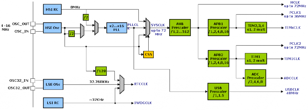
STM32F103 Internal Clock Arrangement (Source: The Insiders Guide to the STM32 ARM based Microcontroller from HITEX, http://www.hitex.com/fileadmin/pdf/insiders-guides/stm32/isg-stm32-v18d-scr.pdf)
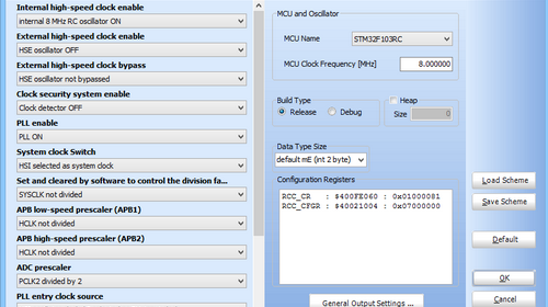
This view give a straight forward insight of the clock hardware. When it comes to software, it is very easy to configure this vast array of hardware. The good stuff about MikroC PRO for ARM and the good news for us is the fact that its IDE already ported an easy-to-use clock configuration tool just as MikroElektronika added fuse configuration tools for its PIC and AVR compilers.
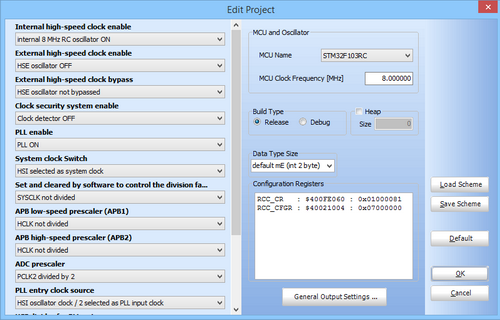
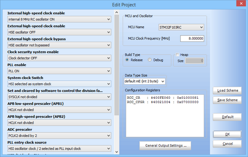
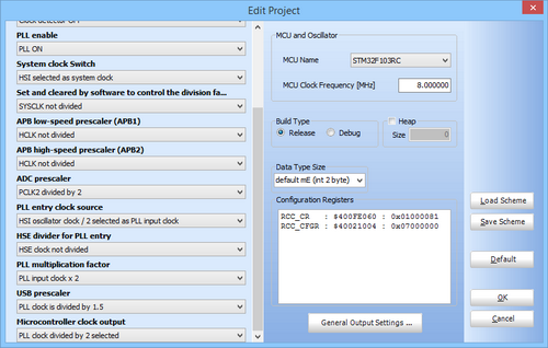
This clock configuration option pops up whenever we start a new project. Alternatively we can go to the Project tab in the MikroC IDE and select Edit Project. If configured properly then it is not needed to manually code clock settings by accessing Reset Clock Control (RCC) registers. In fact we won’t be needing to add the generated values of the RCC registers anywhere in the code. These values are automatically integrated with the user code. However this feature doesn’t limit us to code RCC registers on our own.
Now let’s check out what clock sources are there in a STM32 micro. There are two basic types of clock and they are themselves divided into two speed categories. These are as follows:
- External Sources
- High Speed External (HSE) clock sources can be crystal oscillators, resonators or clock signal generating circuits. When using clock generator circuits, the waveform from such circuits do not necessarily always need to be square waves. HSE accepts sine and triangular waves but whatever waveform is used it must be symmetrical, i.e. 50% on and 50% off and only OSC_IN pin is used to feed the clock signal, leaving OSC_OUT pin open. Typically the HSE of STM32 MCUs accepts clock frequencies from 4 – 25MHz. If external clock circuitry is used then HSE oscillator should be bypassed. This will ensure no conflict.
- Low Speed External (LSE) clock sources share properties similar to HSE sources but usually very accurate 32.768 kHz clock crystals are used to feed the LSE. This is the most profound use of LSE as LSE feeds STM32’s internal Real Time Clock (RTC) module.
- Internal Sources
- High Speed Internal (HSI) clock source is an internal fixed 8MHz clock source. It is factory calibrated and has 1% tolerance.
- Low Speed Internal (LSI) clock source is similar to LSE but it is not very accurate. Typically its frequency is somewhat between 30 – 60 kHz. For most common uses it is considered to have a mean frequency of 45 kHz. Due to such high deviations I strongly recommend not to use it for the internal RTC.
There are prescalars at various points and these can be used to configure individual clocks of various parts of the STM32 MCU. This feature not only ensures energy saving but also aid in running various components of the micro at optimum speeds. An optional clock security unit is also available for use that can switch to HSI should HSE fail for some reason. Apart from different clock sources there is a Phase-Lock-Loop (PLL) module that can multiply either HSE or HSI to generate yet larger values of clock. In fact an 8MHz HSI or HSE clock is passed through the PLL with 9 as multiplying factor to generate full speed 72MHz clock. This also why most ready-made STM32 development boards like the ones I use for demos come with an 8MHz crystal oscillator.
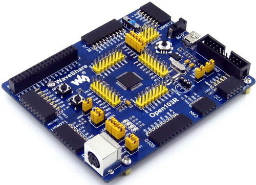
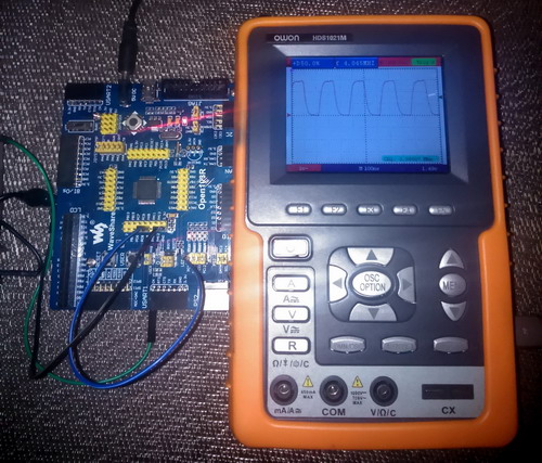
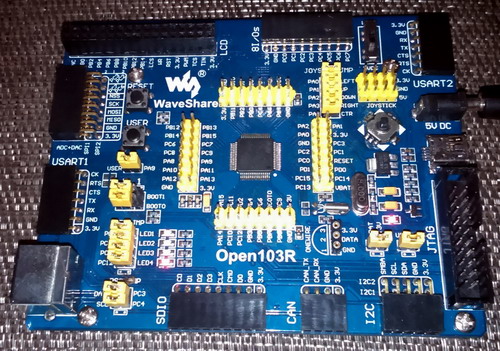
Waveshare’s STM32 development board
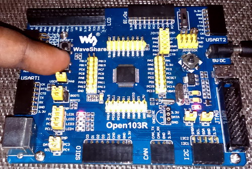
Though out this post I have used a Waveshare’s Open103R STM32F103RC delevopment board – http://www.wvshare.com/product/Open103R-Standard.htm. Like I said about development board and crystal oscillators in them this board also comes with an 8MHz and a 32.768 kHz clock crystal. As much as I have used Waveshare STM32 goods I have come across basically three categories of STM32 ARM development boards. Firstly they have Open series development boards that pack all of the features one might expect in a microcontroller development board and these boards come with easy to interface headers for connecting to external hardware like CAN communication modules, RTC modules, LCDs, etc. Secondly they also have a plug-in-module (PIM) based Open series boards that have minimum hardware and they can used either separately or with an extension motherboard. Thirdly they have Port series boards that are lighter versions of Open series boards.
When dealing with STM32’s clock, there are a few things that need well understanding. The ARM Cortex M3 is a network of instruction/data buses. Fore important buses of the Cortex are the Core System Clock, Advanced High Speed Bus (AHB), Advanced Peripheral Bus 1 (APB1) and Advanced Peripheral Bus 2 (APB2). These buses are connected as such that they are connected to the Direct Memory Access (DMA) module, SRAM, peripherals like GPIOs, ADC, timers, etc. and Cortex core. At present we need just to know about APB buses and they are of the highest importance to us. This is because we are currently dealing with the peripheral hardware of the STM32 micro and certainly not other stuffs like the DMA, Cortex core, etc. It is well known from previous posts that APB1 has a maximum operating frequency of 36MHz while APB2 can run as fast as the AHB bus – 72MHz. You can now understand why GPIOs are connected to APB2 bus instead of APB1 or any other bus and how STM32 GPIOs can achieve 50MHz switching speed. APB1 bus mostly serves communication and timer modules of the STM32. APB1 frequency is not automatically scaled to have half the speed of AHB and so we need to make sure it is not overclocked by mistake. Overclocking is not a good practice and is also not recommended by any manufacturer. To avoid overclocking the APB1 bus always use at least a prescaler of 2 whenever driving the STM32 beyond 36MHz.
Lastly we can also get clock output from a special pin called Microcontroller Clock Output (MCO). The MCO pin is usually located at PA8 pin. However to use the MCO we need to set PA8 as an Alternate Function (AFIO) output. The MCO pin can be used to clock another micro or as a time-base for another circuit or device.
Code Example:
The code example for configuring STM32’s clock and its MCO pin is literally no code at all. Everything is done by the IDE’s clock configuration tool. We’ll just need to configure the MCO pin. In all of the codes in this post, I used MikroC’s GPIO library as it easy to use and saves a lot of time.
void main()
{
GPIO_Clk_Enable(&GPIOA_BASE); //Enable clock for GPIOA
GPIO_Config(&GPIOA_BASE, _GPIO_PINMASK_8, (_GPIO_CFG_MODE_ALT_FUNCTION | _GPIO_CFG_SPEED_50MHZ | _GPIO_CFG_OTYPE_PP)); //Set PA8 as a high speed digital output
while(1)
{
//To do stuffs here
};
}
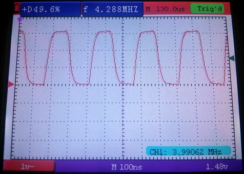
Notice how the clocks are configured. I used the HSI and didn’t use the HSE. I use HSI just to show its accuracy. I used PLL as such that the 8MHz HSI is first divided by 2 before entering the PLL stage. Thus the PLL gets 4MHz input and it then multiplies this value with 2 to generate 8MHz clock. Finally The MCO outputs a clock signal of half the value of the PLL output, i.e. 4MHz. The STM32 core however runs using HSI instead of the PLL. An oscilloscope hooked with the MCO pin registers that the clock out has a frequency of 3.99MHz. It is close enough for most applications. This is the simplest demo I could imagine.
Video link: https://www.youtube.com/watch?v=Fgbju2Qznkw
Independent Watchdog
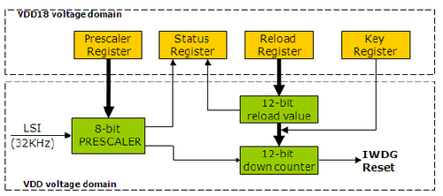
As the name suggests the Independent Watchdog (hereinafter referred as IWDG) is a completely independent watchdog timer. It has separate dedicated clock and it remains operational even if the main clock of a STM32 micro fails. Thus IWDG is suited especially for those applications where it is needed just to reset a STM32 MCU on failure or due to a hang up. This is just like the regular watchdog timer use in common 8 bit MCUs. There is nothing complex about it.
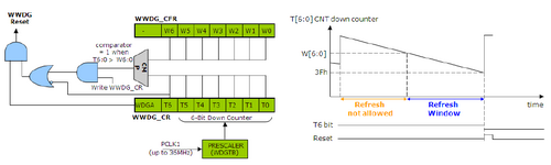
The dedicated separate clock of the IWDG hardware comes from Low Speed Internal (LSI) clock. It is not an accurate one as one might expect. This inaccuracy is due to the fact that the LSI is a RC oscillator. It has an oscillation frequency of somewhat between 30 – 60 kHz. For most applications it is assumed to have a mean frequency of 45 kHz though it is supposed to be around 32 kHz. This assumption makes it simple although there will be some deviation. Shown below is the internal block diagram of IWDG hardware:
There are a few registers associated with IWDG and the register map for IWDG is shown below:
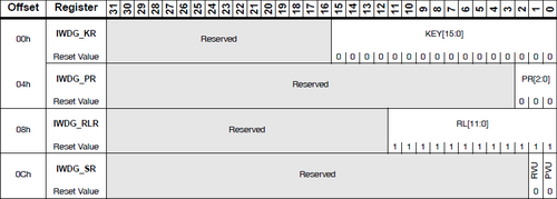
Activating the IWDG is straight. All we need to do is to load the Key Register IWDG_KR with a predefined constant 0xCCCC. Once loaded with this value the IWDG hardware is initiated and its counter will down count from a reset value 0xFFF or a preloaded value to 0x000. When the counter counts to 0x000 count, a reset signal is issued. This is normally what we will not be wanting and so to avoid the reset we need to rewrite IWDG_KR with 0xAAAA. This will reload the counter and thus reset is avoided. At this point it is pretty much clear that we will periodically need to write 0xAAAA to the IWDG_KR register in the software. Should the software get stuck it will not be doing so and when time or count runs out, the IWDG will restart the MCU right from the initialization stage.
Before we activate the IWDG it should be configured according to our timeout need. The IWDG_PR and IWDG_RLR registers hold prescalar or divisor factor and reload values respectively. These values decide the required timeout before reset. These registers are by default write protected and so to alter their values we need to follow a sequence or otherwise write protection will not be removed. To configure the IWDG, we need to follow according to the steps below:
- Load IWDG_KR register with 0x5555. This will remove write protection for IWDG_PR and IWDG_RLR registers, allowing us to edit their values.
- Edit values for IWDG_PR and IWDG_RLR registers.
- Enable write protection by issuing reload command, i.e. writing 0xAAAA to IWDG_PR register.
- Start the IDWG by loading IWDG_PR with 0xCCCC.
The formula for IWDG timeout is as follows: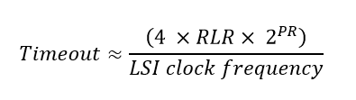
If, for example, RLR equals 180, PR equals 6 and the LSI has a frequency of 45 kHz then we roughly get a timeout of about 1000ms or 1s.
Code Example:
The code example for IWDG and the setup for it is very simple. A LED connected to PC 9 remains off until a push button connected to PA9 is pressed. This indicates initialization stage. Once pressed and held, the LED starts blinking, indicating normal operation. When the button is released, the LED stays on and then goes to reset after about one second. We, then, know for sure that the STM32 went to reset by seeing that the LED is turned off as it was during start up.
/* Function prototypes */
void setup();
void setup_GPIO();
void setup_IWDG();
void main()
{
setup();
while(1)
{
if(GPIOA_IDRbits.IDR9 == 0) //If the switch is pressed
{
GPIOC_BRRbits.BR9 = 1; //Turn off LED
delay_ms(90); //Wait for 90ms
GPIOC_BSRRbits.BS9 = 1; //Turn on LED
delay_ms(90); //Wait for 90ms
IWDG_KR = 0xAAAA; //Reload IWDG
}
};
}
void setup()
{
setup_GPIO();
setup_IWDG();
while(GPIOA_IDRbits.IDR9 == 1); //Wait till the switch is pressed
}
void setup_GPIO()
{
GPIO_Clk_Enable(&GPIOA_BASE); //Enable clock for GPIOA
GPIO_Clk_Enable(&GPIOC_BASE); //Enable clock for GPIOC
GPIO_Config(&GPIOA_BASE, _GPIO_PINMASK_9, (_GPIO_CFG_MODE_INPUT | _GPIO_CFG_PULL_UP)); //Set PA9 as a digital input with pull-up
GPIO_Config(&GPIOC_BASE, _GPIO_PINMASK_9, (_GPIO_CFG_MODE_OUTPUT | _GPIO_CFG_OTYPE_PP | _GPIO_CFG_SPEED_2MHZ)); //Set PC9 as a digital output
GPIOC_BSRRbits.BS9 = 0; //Turn off LED
}
void setup_IWDG()
{
IWDG_KR = 0x5555; //Disable write protection of IWDG registers
IWDG_PR = 0x06; //Set PR value
IWDG_RLR = 0xB4; //Set RLR value
IWDG_KR = 0xAAAA; //Reload IWDG
IWDG_KR = 0xCCCC; //Start IWDG
}
Video link: https://www.youtube.com/watch?v=_6VAUcnRPVM.
Window Watchdog
The Window Watchdog (WWDG) is an advanced watchdog timer concept. It can detect if a program is executing earlier or later than a predefined time window. Using this info it can understand if things are working perfectly or not and reset a STM32 micro if things are not okay. Unlike the IWDG or the usual watchdog timerconcept where just a counter is monitored and reloaded periodically, the WWDG is reloaded or refreshed within the predefined time window (referred just as window from now on), reloading it earlier or later than what was defined as time frame will result in a reset. Thus the WWDG is helpful in debugging software bugs apart from other uses.
Windowed Watchdog (Source: The Insiders Guide to the STM32 ARM based Microcontroller from HITEX, http://www.hitex.com/fileadmin/pdf/insiders-guides/stm32/isg-stm32-v18d-scr.pdf)
The WWDG will start its counter after setup and will down-count from a preset top value to the window value and so forth. A reset will occur when its counter counts from 0x40 to 0x3F, i.e. when the T6 bit of WWDG_CR is cleared. A programmer can only set the upper value of the window and that is because the lower value is 0x40. At 0x40 count, the WWDG will give an early wakeup call in the form of an interrupt because after this at 0x3F count it will reset the STM32 CPU. As shown in the block diagram above, window (W) bits are compared with counter (T) bits. The W bits are unaltered after setting them during initialization because these bits hold the value of the count after which we are allowed to reload the down counter or T bits. ST recommends that WWDG_CR is either configured as 0xFF or 0xCC. Doing so will ensure that the counter starts counting well above what’s stored as window. I suggest that are set as 0x7F as it is the maximum possible value. I recommend so to avoid unnecessary minor overlooking and head-scratching mistakes.
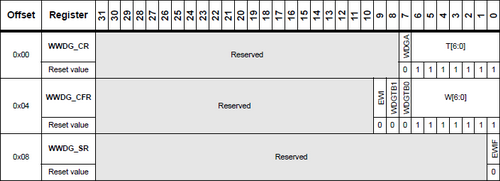
Like the IWDG, the WWDG also has few registers to configure. Here’s the register map for WWDG:
To use the use the WWDG, we need to follow the following steps as given in the order below:
- Unlike the IWDG which has its separate clock, the WWDG’s clock input comes from APB1 bus and so just like enabling clocks for GPIO ports or any other bus-driven hardware we need to enable the clock for WWDG. This is done by setting the 11th bit (WWDGEN bit) of the RCC_APB1ENR register.
- After enabling clock for the WWDG, we need to configure the WWDG_CR and WWDG_CFG registers along with clearing interrupt flag. Configuring these registers will configure the timing parameters like the window, prescalar, initial counter value and of course enable the WWDG. One thing to note at this point is the fact that after the WWDG is enabled in the software, it cannot be disabled without a reset.
- Finally if we need to use the WWDG early wakeup interrupt (EWI), we’ll need to configure the NVIC for that. I strongly suggest using this interrupt as it will run in the background and thereby needing no attention during coding. Should there be some problem with the software execution, it will automatically the reset the CPU, requiring no user intervention.
- In the interrupt we need to clear the interrupt flag but clearing WWDG_SR register’s EWIF bit. We will also need to reload the counter.
Before going further there are some certain points I must clear first because ST’s documentation is somewhat a bit confusing. The window value and the counter values are both 7 bits wide. However please notice the formula below for obtaining WWDG timeout:
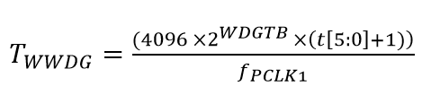
Notice that the counter value t is shown to be 6 bits wide instead of 7 bits. To make things clear, first consider that to be 0, the window value to be 95 (0x5F) and the counter’s initial value to be 127 (0x7F). From 127 to 95 counts we cannot refresh the WWDG counter as doing so will cause a reset. Between 94 to 64 counts we can reload the WWDG counter. If, for example, is 36MHz and is 3 then is 910µs. Thus each count takes this much time. Hence the refresh window is between to . Reloading the counter before 29.13ms or reloading it after 58.25ms will result in reset.
Code Example:
In this demo example for the WWDG, I used a pair of LEDs designated WWDG LED and main LED. The WWDG LED is connected to PC9 and main LED is connected to PC12. There is also a button connected to PA9. What happens in the code is pretty simple. The entire working of the WWDG is handled by its ISR. When the code starts the main LED turns on and the WWDG LED is held off at the same time. This indicates the starting of the code. After this the main LED toggles every 300ms while the WWDG LED also toggles but at a much faster rate than the main LED. The WWDG LED’s toggling suggests that it has reached early wakeup count by down counting from initial value and the WWDG counter is being reloaded. The main LED toggles as to show that normal operation are going on okay. If however the button is pressed, the counter is forced to zero, causing a WWDG reset. The process repeats once the button is released and the whole thing starts over again.
/* Function prototypes */
void setup();
void setup_GPIO();
void setup_WWDG();
void WWDG_ISR()
iv IVT_INT_WWDG ics ICS_AUTO //WWDG early wakeup interrupt function
{
unsigned char cnt = 0; //Temporary variables for counter and window values
unsigned char wdt = 0;
wdt = (WWDG_CFR & 0x7F); //Read window value
cnt = (WWDG_CR & 0x7F); //Read counter value
if(cnt < wdt) //If counter is less than window value
{
WWDG_CR |= 0x7F; //Reload the counter
WWDG_SR = 0x00; //Clear interrupt flag
GPIOC_ODRbits.ODR9 ^= 1; //Toggle WWDG LED
}
}
void main()
{
setup();
while(1)
{
GPIOC_ODRbits.ODR12 ^= 1; //Toggle main LED
delay_ms(300); //Wait for 300ms
if(GPIOA_IDRbits.IDR9 == 0) //If button is pressed
{
WWDG_CR = 0x80; //Force the counter to zero
while(1); //Get stuck into an infinity loop
}
};
}
void setup()
{
setup_GPIO();
setup_WWDG();
}
void setup_GPIO()
{
GPIO_Clk_Enable(&GPIOA_BASE); //Enable clock for GPIOA
GPIO_Clk_Enable(&GPIOC_BASE); //Enable clock for GPIOC
GPIO_Config(&GPIOA_BASE, _GPIO_PINMASK_9, (_GPIO_CFG_MODE_INPUT | _GPIO_CFG_PULL_UP)); //Set PA9 as a digital input with pull-up
     GPIO_Config(&GPIOC_BASE, (_GPIO_PINMASK_9 | _GPIO_PINMASK_12), (_GPIO_CFG_MODE_OUTPUT | _GPIO_CFG_OTYPE_PP | _GPIO_CFG_SPEED_2MHZ));
                                          //Set PC9 and PC12 as digital outputs
GPIOC_ODRbits.ODR9 = 0; //Turn off WWDG LED at first
GPIOC_ODRbits.ODR12 = 1; //Turn on main LED at first
delay_ms(1000); //Wait for a second
}
void setup_WWDG()
{
RCC_APB1ENRbits.WWDGEN = 1; //Enable clock for WWDG module
WWDG_CFR = 0x3DF; //Set WWDG_CFR register
WWDG_SR = 0x00; //Clear interrupt flag
WWDG_CR = 0xFF; //Turn on WWDG and load the counter
NVIC_IntEnable(IVT_INT_WWDG); //Enable NVIC for WWDG interrupt
EnableInterrupts();
}
Video link: https://www.youtube.com/watch?v=E8_S2qKagDM.
It is also possible to halt both the IWDG and WWDG to halt during STM32 debugging session using the STM32’s MCUDBG register. With this feature unnecessary resets during a debug session can be avoided when STM32 core is halted.
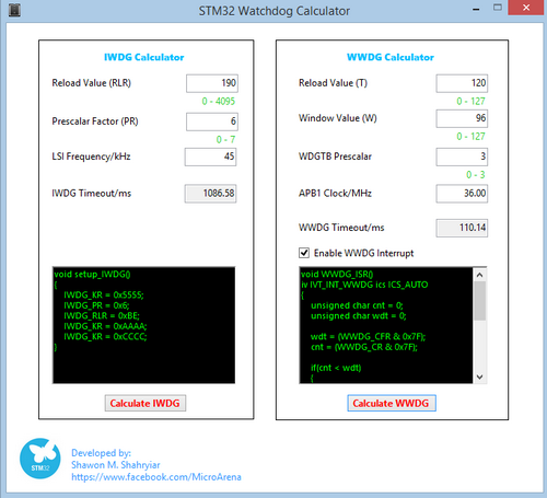
For making things easy, I have designed a GUI that can calculate parameters and generate code for both the IWDG and the WWDG. Here is a screenshot of the GUI in action.
To summarize:
- STM32’s clock options are agile and flexible. There are various ways to achieve optimum clocking. Please refer to the RCC section of the STM32 reference manual for details.
- Without fully realizing the STM32 clock peripheral it is pointless to go any further.
- I personally recommend using the HSE for accurate timing although HSI is good enough for most applications. 1% deviation of frequency due to tolerance of the HSI is not a big deal.
- I don’t recommend using LSI anywhere other than for the IWDG hardware. A very accurate 32.768 kHz clock crystal should be used for the LSE if it is to be used for the internal RTC.
- It is not always necessary to run any MCU at max oscillator frequency as a higher operating frequency needs higher energy. This is what we should avoid if we are to design battery-operated or energy efficient devices.
- IWDG and WWDG are different types of watchdog and should be deployed according to specific requirement. IWDG and WWDG are not interchangeable by any means.
Files: STM32 Internals.
References:
The Insiders Guide to the STM32 ARM based Microcontroller from HITEX, http://www.hitex.com/fileadmin/pdf/insiders-guides/stm32/isg-stm32-v18d-scr.pdf
I wish readers a useful STM32 experience. Happy coding.
Repository: https://github.com/sshahryiar/STM32-Tutorials
Author: Shawon M. Shahryiar
https://www.youtube.com/c/sshahryiar
|
|
hello thanks again for this tutorial but i am somehow confused are you saying i can get up to 72mhz even with an
8mhz external crystal oscillator because my development board comes with an 8mhz crystal osccilation so tell me if am right say i want 48mhz can i achieve this by setting hse on,pll on,select pll as system clock,set pll multiplication factor to x6 to get 48mhz
Yeah you are right…. 8MHz x 6PLL = 48MHz….
Pingback: Down the Rabbit Hole of STM32 Clock Options | Hackaday