EasyESP-1: A rapid prototyping and development board for ESP8266
|
|
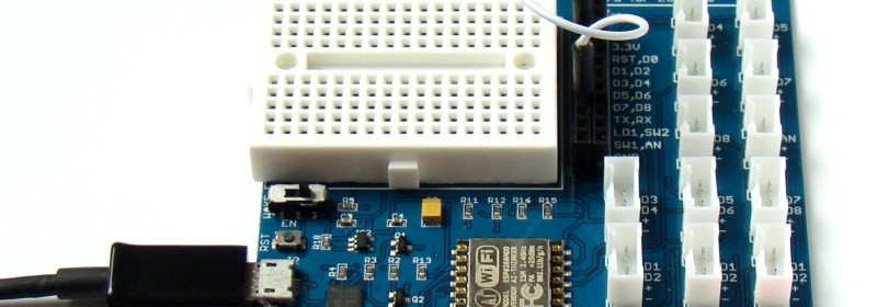
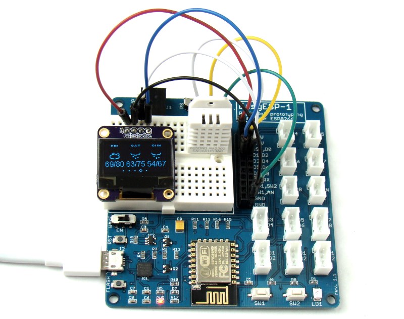
EasyESP-1 is a rapid prototyping development board for the low-cost, WiFi-enabled ESP8266 microcontroller. With an onboard USB-to-Serial converter pre-installed, EasyESP-1 does not require any additional hardware to download your application firmware to the ESP8266 chip. The ESP module used in this development board is ESP-12E. All the I/O pins are broken out to 0.1” female headers for easy access, as well as to standard Grove connectors for connecting Grove sensors and other compatible modules. The 180-point breadboard further facilitates experimenting and testing of external circuits. You can buy EasyESP-1 from our Tindie Store. Non US buyers can also get it from Elecrow.
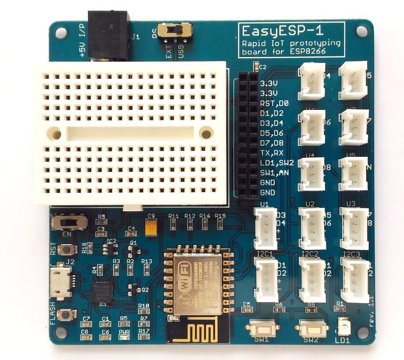
Fig. 1: EasyESP-1 development board
List of features
- Easy access to all GPIO pin through female headers and Grove connectors
- On-board USB-UART chip for easy programming and debugging
- 180-point breadboard for experimenting with test circuits
- On-board 3.3V (800 mA) regulated power supply
- Two tact switches for user inputs, and one output LED
- Slide switch to enable/disable auto Wake Up feature during Sleep mode
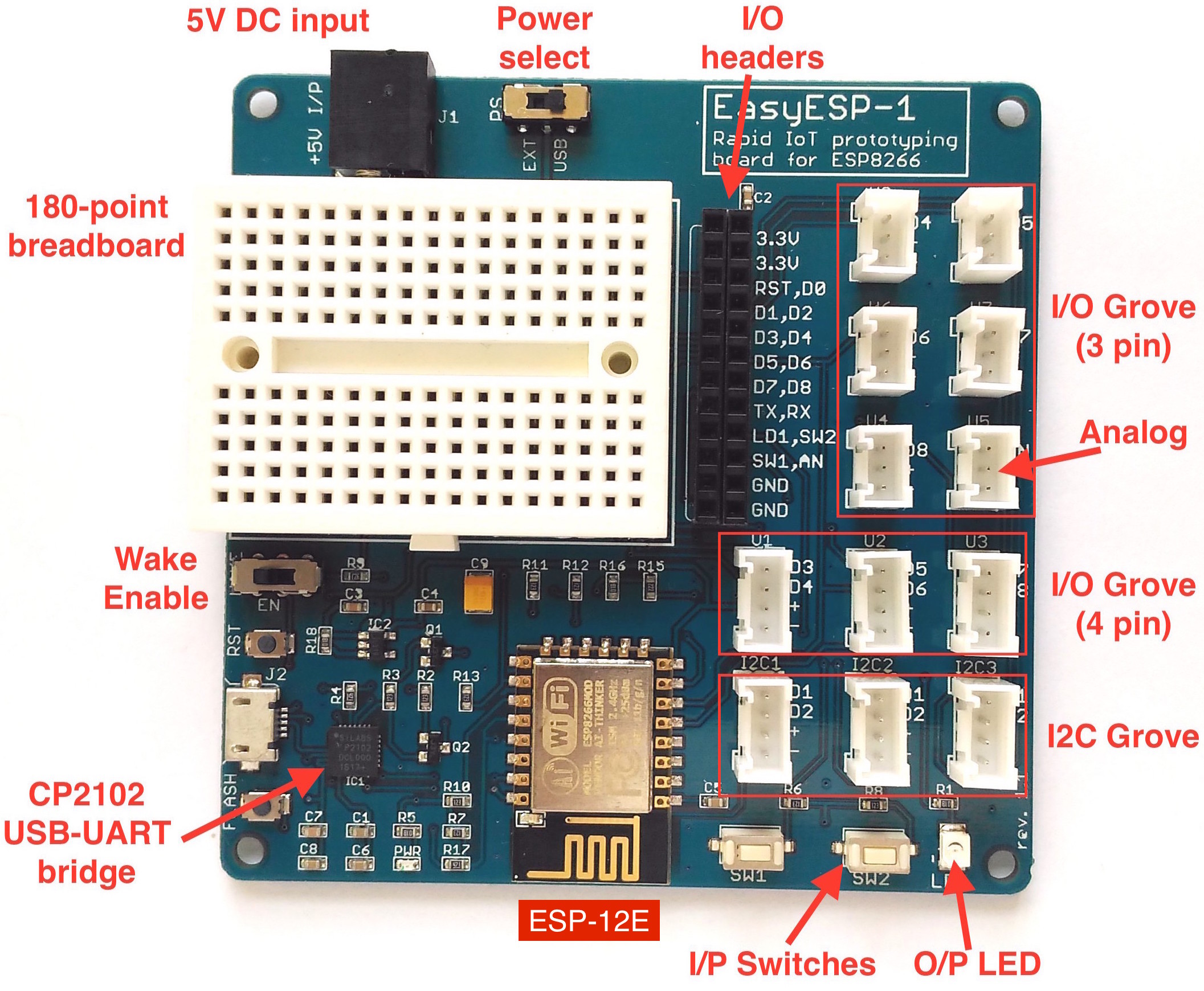
Fig. 2: EasyESP-1 features
Power supply
The ESP8266 module operates at 3.3V power supply. The EasyESP-1 derives the 3.3V power supply for the ESP12E module from the USB port or an external 5V DC input using the SPX3819 low-noise LDO voltage regulator. The maximum current capacity of the LDO is 500mA. There is a power select (PS) slide switch (see Fig. 2) to switch between the USB and the external 5V power supply options. During programming, the EasyESP board is connected to the PC’s USB port, so it is convenient to use the USB power supply. The PS switch must be in the USB position in order to use the USB power source. If you need to use an external power supply for any reason, you will need a regulated +5V DC with minimum current rating of 500mA (1A recommended) and with a 2.1mm male output power plug. The external power supply plugs into the input DC barrel jack next to the PS switch. Note that the PS switch must slide to the EXT position in this case.
Note: Remember, the external DC input should be a regulated +5V.
CP2102 USB-UART bridge
EasyESP-1 uses Silicon Labs’ CP2102 USB to serial bridge device on board for uploading user applications to the ESP module. It also allows the users to use a serial terminal program (such as serial monitor on Arduino IDE) on a computer for debugging. Drivers for this USB-UART bridge device can be downloaded from Silicon Labs website.
I/O peripherals
The I/O pins of ESP12E module are broken out to 0.1″ pitch female headers (J3), as well as to multiple grove connectors. The ESP12E I/O pins that are available on the board are RST, D0-D8, Tx, Rx, and analog input pin AN. The built-in ADC of ESP8266 has 10-bit resolution and can accept an input voltage ranging from 0 to 1.0V. In order to expand the range of input analog voltage to 3.3V, EasyESP-1 incorporates a simple 2-resistor voltage divider network as shown in Fig. 3.
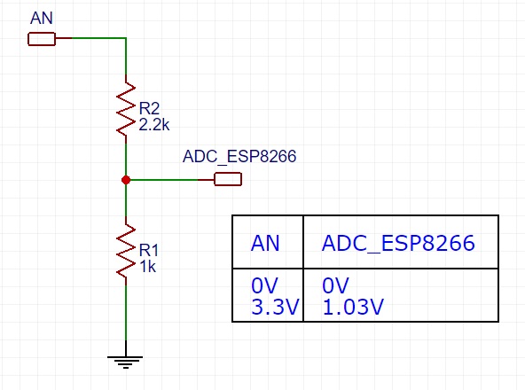
Fig. 3: A resistor divider network increases the range of ADC input to 3.3V
The two user tact switches (SW1 and SW2) and one user LED (LD1) are also accessible through female headers (J3). The tact switches output are pulled up “High” during default conditions. When they are pressed, the corresponding J3 pins (SW1 and SW2) turn “Low”. Similarly, LD1 is configured as active high, which means when the LD1 pin of J3 is connected to logic “High”, the LD1 LED turns on. All ESP12E I/O pins, user tact switches and LED, and power supply pins are arranged in a 2×12 header (J3). The AN pin is also accessible through U5 grove connector. In ESP8266, I2C is implemented by bit-banging, and as such, any two I/O pins can be configured as I2C bus. However, to make it easier for the users, the EasyESP-1 board provides three I2C grove connectors (I2C1, I2C2, and I2C3) that are hard-wired to D1 (SCK) and D2 (SDA) pins. A close-up picture of just the I/O section of EasyESP-1 is given in Fig. 4.
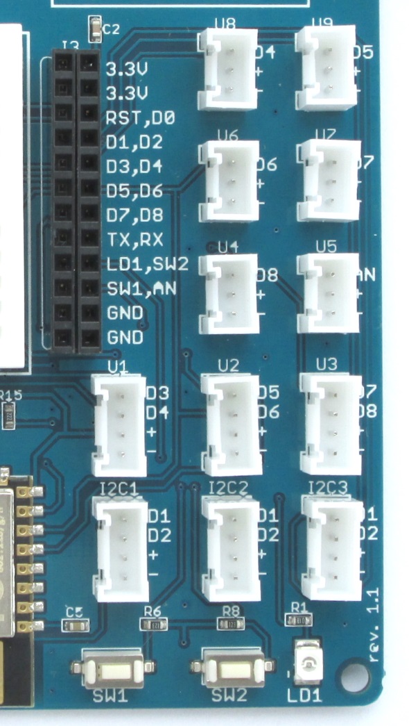
Fig. 4: A 2×12 female header (J3) and grove connectors provide access to the ESP12E I/O pins and the user switches and LED
It should be noted that EasyESP-1 uses the same I/O indexing as used by NodeMCU. This does not match with internal GPIO indexing. For example, pin D1 is actually mapped to internal GPIO5. If you use Arduino IDE for programming EasyESP-1, you can access this pin in both ways. For instance, digitalWrite(D1, LOW) and digitalWrite(5, LOW) will both do the same thing, writes out logic ‘low’ to D1 pin. Following diagram describes the pin mapping between EasyESP-1 Dx and ESP8266 internal GPIOs. Note that TX and RX pins can also be called for normal I/O operation by addressing them as D10 (GPIO1) and D9 (GPIO3), respectively.
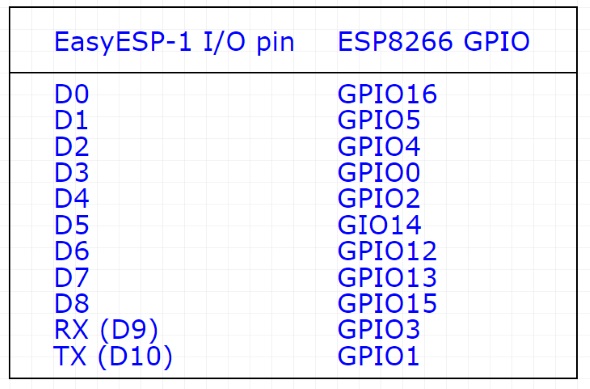
EasyESP-1 I/O pin indexing vs ESP8266 internal GPIOs
Wake Enable switch
For low-power applications, ESP8266 can be put into deep sleep mode during idle conditions. In order for the ESP8266 to automatically wake up from sleep mode after a certain interval, the XPD/D0 pin (which is also GPIO16) must be tied to the ESP8266’s reset line. In EasyESP-1 board, this can be easily done by sliding the Wake Enable switch to EN position.
Download EasyESP-1 Eagle CAD files
Buy EasyESP-1 from our Tindie Store
International buyers visit here
ESP8266 experimenting made easy with EasyESP-1
|
|
Pingback: EasyESP-1: A beginner's prototyping board for ESP8266 - Electronics-Lab
Pingback: A rapid prototyping and development board for ESP8266 - Electronics-Lab