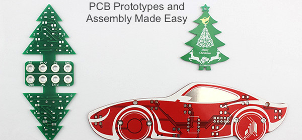
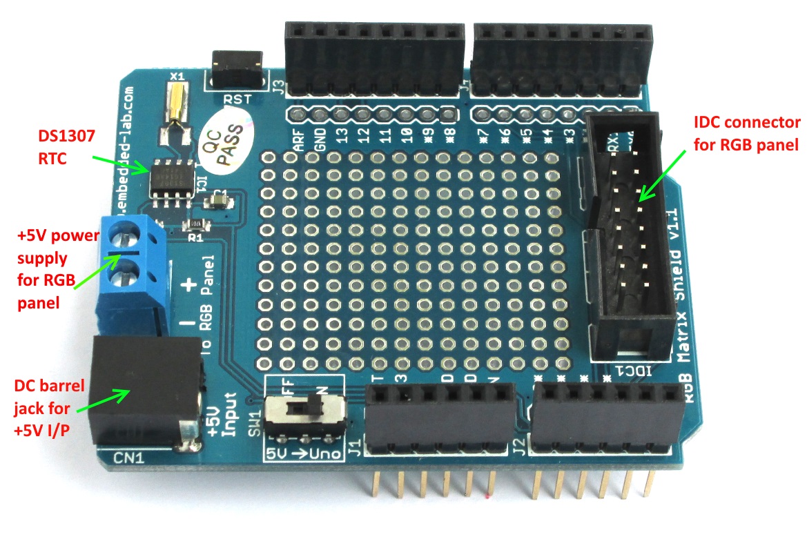
Printed Circuit Boards – Things You Must Know as a Beginner
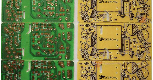
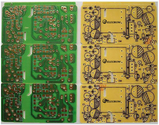
A systematic arrangement of electrical components defined by pathways, signal traces, and conductive paths is called a Printed Circuit Board. If as a beginner you question, ‘what’s a PCB?’, then for simpler understanding, you can look at a PCB this way. Functionally speaking, the PCB offers mechanical support to electrical connections arranged in a logical manner with the help of pads, tracks, and other features. You can find the best PCBs at a cheap PCB manufacturer such as Elecrow.
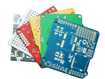
Types of PCB
PCBs can be categorized as follows:
- Single Sided PCBs
- Multilayer PCBs
- Double Sided PCBs
- Flex PCBs
- Rigid PCBs
- Rigid-Flex PCBs
Single Sided PCBs
This single sided printed circuit board includes a single layer of the substrate. Either side of the substrate is coated with a good conducting material, such as copper. It is made by applying a protecting solder cover on the top layer of the copper substrate. Additionally, a silkscreen coating is done to define the mark elements of the board.
This is the most easily made PCB and as a beginner, you may be given a task to learn this first before trying hands on more complex types of PCBs. All components and circuits are demarcated on the single side, providing a suitable ground for easy electronics. These can be produced in large numbers but do not find much utility due to limited design options available in these.
Double Sided PCBs (2 layer PCB)
In these PCBs, both sides of the substrate are used for placing elements. The placement of elements is done with the help of surface mount or through hole technology. Its structure is quite similar to single sided PCBs w the only difference being that both sides of the substrate are employed.
Multi-layer PCBs
These PCBs are quite useful for creating complex and thick designs. The layers are added both to the top as well as bottom in the configuration of double-sided. The additional layers act as power planes that do the dual function of providing supply to the circuit and of decreasing the electromagnetic interference. The EMI levels can be lowered further by using the middle portion of these power planes.
Rigid PCBs
PCBs are also available in varying rigidities. In addition to adding layers, PCBs are also designed keeping flexibilities in mind. A motherboard inside a computer tower is the most common example of a rigid PCB. The rigid PCB is characterized by a substrate made of fiberglass that keeps the board from bending or twisting.
Apart from these, Flex PCBs and rigid-flex PCBs from Elecrow Premium PCB service are also manufactured in order to meet the requirements of different kinds of environments. For example, flexible PCBs are used in environments such as satellite gears, which are exposed to a lot of twisting and shifting.
Principle of PCB Layout
1. PCB layout guidelines suggest that the structure of this board should meet the following requirements: Traces carrying currents should be amply thick;
- Traces carrying currents should be amply thick;
- The board should support low impedance;
- Signals of sensitive type should be able to stop interference caused by noisy traces.
Thus, PCB Layout Guidelines entail the use of plane shapes wherever possible. These shapes support high current input supplies such as DCIN, VBAT, and VBUS. Plane shapes deliver the benefit of cutting on power losses. The continuous flow of current between the layers is to be ensured and this is provided by the plane shapes. To achieve this, the plane is not to be interrupted or shortened too much by vias.
Another guideline is to maximize the productivity of decoupling capacitors. This is done by minimizing the inductance between the capacitor and the power pin of any device. To achieve this, the capacitor is placed closest possible to the device. Traces should be short and thick, and the vias should not have inductive element if you want to enhance the effectiveness of decoupling capacitors. Similarly, the capacitor and ground should be connected in low impedance manner so that the impedance of the former can be minimized. To further reduce the ground impedance, the unused areas of PCB should be flooded with the ground.
2. The grounding of PCBs is another factor that constitutes the guidelines for ensuring better efficiency of the circuit board. There are two types of layouts prevalent – star grounding and ground looping. Of these, star grounding performs better and delivers minimum impedance.
Ground loopings cause the disturbed flow of current across different layers. These loopings need careful identification especially in multi-layer boards for avoiding duplication and fault.
3. Placement of external components: The external components like reference-setting components should be placed near to each other. It can also be achieved by switching inductors and capacitors with their drive-pin components. The layout of sensitive parts and high current devices should be given topmost preference, in order to ensure better system performance.
Guidelines are also laid for the placement of boards in correct proximity to the power source, ADC, etc.
How do circuit boards work
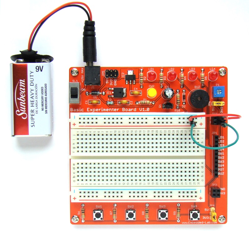
This is how circuit boards work. The electronic components are connected electrically using pads, conductive tracks and other features peeled from the copper sheets. The circuit boards also provide mechanical support to these components. All basic components such as resistors, capacitors and other active devices are fixed on the PCB by the way of soldering.
Circuit boards are, therefore, simple in design, easy to work and can be made from basic materials such as copper boards and basic kinds of electronic components. These form the core of internal networks present inside computers, or other electronic devices.