Exploring the chipKIT Uno32 board
|
|
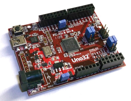
The chipKIT Uno32 development board is based on the powerful PIC32MX320F128 microcontroller, which features a 32-bit MIPS processor core running at 80MHz, 128K of flash program memory, and 16K of SRAM data memory. The board can be powered via USB or an external power supply. The on-board USB-UART interface provides a communication path between the board and the MPIDE tool running on the PC. MPIDE stands for Multi-Platform Integrated Development Environment and is a complete tool for developing and downloading embedded applications into the chipKIT Uno32 board. Now let’s explore the chipKIT Uno32 board and its on-board features in more detail.

chipKIT Uno32 board
The complete description of the chipKIT Uno32 board can be found in its hardware manual available from the Digilent’s website. I am summarizing only the most important features here. Shown below is a picture, drawn by me, that shows the layout of the major components, jumpers, and connectors on the chipKIT Uno32 board.

Layout of the major components, connectors, and jumpers
Connection to PC
The Uno32 board uses a standard Mini-B USB connector for connection to a USB port on the PC. The FTDI FT232RQ chip next to the USB connector provides an USB-UART interface for a two-way serial communication between the PC and the board. The same serial port is used by the MPIDE to communicate with the serial bootloader running on the Uno32 board while downloading user applications.
Power supply section
The Uno32 can be powered either via USB or from an external power supply. The automatic switch-over circuit on-board causes the external supply to be used if both supplies are present. There are two voltage regulators present in the Uno32 board. The first regulates the external supply voltage to 5V and powers the +5V bus line (VCC5V0) on the board. The second regulates the VCC5V0 bus to 3.3V that goes to the 3.3V bus (VCC3V3) and also powers the PIC32 microcontroller. A 5.5 mm x 2.1 mm barrel connector is available to power the Uno32 board from an external power supply (wall adapter). The center terminal of the connector is wired as the positive supply voltage. The external power supply voltage must be in the range 7V to 15V.
Jumper JP2 provides an option to route the external power supply voltage through the on-board 5V regulator or directly to the VCC5V0 bus, bypassing the on-board 5V regulator. Normally, JP2 is in the REG position. This routes the external supply through the 5V regulator. If the external power supply is already a regulated +5V output, JP2 can be placed in BYP position to power the VCC5V0 bus directly from the external source.
The 6-pin POWER connector, J2, is used to power external circuits or shields connected to the Uno32 board. Pin 1 (RESET) is connected to the MCLR pin on the PIC32 microcontroller. This pin can be used to reset the PIC32 from an external circuit. The second and third pins provide 3.3V (maximum current 425 mA) and 5.0V (maximum current 900 mA) output, respectively, to power an external circuit or a shield plugged into the Uno32 board. The total current provided by pins 2 and 3 together, however, shouldn’t exceed 925 mA. Pins 4 and 5 (GND) provide common ground connections between the Uno32 and any external circuit. Pin 6 (VIN) is connected to the input of the external power supply connector. This pin can be used to provide the unregulated input voltage to the external circuit or the shield connected to Uno32.
Digital I/O pins
The chipKIT and Arduino systems both use logical pin numbers to identify digital I/O pins. The valid logical pin numbers for the Uno32 board are 0-43. The chipKIT Uno32 board provides altogether 42 I/O pins that are accessible through connectors J5, J6, and J7. Each I/O pin can source or sink a maximum of 18mA. However, to keep the output voltage within the specified voltage range (VOL = 0.4V, VOH = 2.4V), the pin current must be restricted to source and sink at most 7mA and 12mA, respectively. The maximum current that can be sourced or sunk across all I/O pins simultaneously is 200mA.
Connectors J5 and J6 are 2×8 female pin header connectors that provide access to 30 I/O pins. The outer row of pins (labeled 0 through 13, A, and G) corresponds to the I/O connector pins on an Arduino Uno board. The inner row of pins (labeled 26 through 41) are the extra I/O signals provided by the chipKIT Uno32.
Similarly, connector J7 is a 2×6 female pin header that provides access to the analog input pins on the PIC32 microcontroller. The outer row of pins corresponds to the six analog pins (A0-A5) on an Arduino Uno board, whereas the inner row of pins are the additional analog channels (A6-A11) provided by the Uno32. These analog pins can also be used as digital I/O pins. In that case, the logical pin numbers of A0-A11 would be 14-25.
So the total 42 I/O pins are distributed as follows:
- Outer row of J6 and J5 -> 14 pins (logical pin numbers 0-13)
- Outer row of J7 -> 6 pins (logical pin numbers 14-19)
- Inner row of J7 -> 6 pins (logical pin numbers 20-25)
- Inner row of J6 and J5 -> 16 pins (logical pin numbers 26-41)
The pin labeled as A on J5 is used to provide an external reference voltage for the microcontroller’s A/D converter. But it can also be used as a digital I/O pin, and its logical pin number is 42.
Pulse width modulation (PWM) pins
The I/O pins 3, 5, 6, 9, and 10 can also be configured to provide PWM outputs.
LEDs on the board
There are 5 LEDs (labeled as LED1 through LED5) on the chipKIT Uno32 board. LED1 and LED2 are communication status LEDs and they will blink when data is being sent or received between the
Uno32 and the PC over the serial connection. LED3 is located next to the barrel connector for external DC supply, and is basically the power-on indicator LED. The Uno32 board has two user LEDs, labeled LED4 and LED5, that are connected to digital I/O Pins 13 and 43. It should be noted that Pin 43 only goes to LED5 and not any connector pin. Driving the pin high turns LED5 on, driving it low turns it off.
Peripheral functions
The PIC32 microcontroller on the Uno32 board provides a number of peripheral functions. The following peripherals are provided:
- Asynchronous serial communication ports: There are two UART ports (UART port1 and UART port2) available on the Uno32 board. Pin 0 and Pin 1 serves as RX and TX for UART port1 and are also connected to the FT232R USB-to-Serial converter on board. It is possible to use these pins to connect to an external serial device when not using the USB serial interface. This uses UART1 (U1RX, U1TX) on the PIC32 microcontroller. Similarly, UART port2 uses Pin 39 and Pin 40 for RX and TX functions respectively. This uses UART2 (U2RX, U2TX) on the PIC32 microcontroller.
- Serial Peripheral Interface (SPI): SPI requires four signal lines (SS-slave select, MOSI-master output slave input, MISO-master input slave output, and SCLK-serial clock) to perform a full duplex communication between a master and a slave. These are provided by Pin 10 (SS), Pin 11 (MOSI), Pin 12 (MISO), and Pin 13 (SCK) on the Uno32 board. These signals also appear on connector J8, which may be used by some shields to access the SPI bus. Jumpers JP5 and JP7 are used to select whether the Uno32 operates as a Master (transmit on MOSI, receive on MISO) or a Slave (transmit on MISO, receive on MOSI) device. The shorting blocks on JP5 and JP7 are normally placed in the Master position for the Uno32 to function as an SPI master. Also, jumper JP4 is used to select PWM output or the SPI SS function on Pin 10. The jumper on JP4 should be in the RD4 position to select PWM output. It should be in the RG9 position to select the SPI SS function.
- Inter-Integrated Communication (I2C): The PIC32 microcontroller shares the analog input pins A4 and A5 with the two I2C signals SDA and SCL. Jumpers JP6 and JP8 are used to select whether the analog pin functions or the I2C pin functions are being used. The shorting blocks are placed in the A4/A5 position to select the analog input function or general digital I/O. They are placed in the RG3/RG2 position to use the pins for I2C operation. This uses I2C1 (SDA1, SCL1) on the PIC32 microcontroller.The I2C bus uses open collector drivers to allow multiple devices to drive the bus signals. This means that pull-up resistors must be provided to supply the logic high state for the signals. The Uno32 board does not have any pull-up resistors for the I2C bus and therefore, must be provided externally.
- External Interrupts: The five external interrupt pins of the PIC32 microcontroller are accessible through Pin 38 (INT0), Pin 2 (INT1), Pin 7 (INT2), Pin 8 (INT3), and Pin 35 (INT4).
- Real time clock calender (RTCC): The PIC32 microcontroller contains an RTCC circuit that can be used to maintain time and date information. The operation of the RTCC requires a clock frequency of 32.768Khz. A space is provided (X2), just above and to the right of the PIC32 microcontroller IC, to solder a 32Khz watch crystal.
- RESET: A reset button is available at the upper left corner of the board. Pressing this button resets the PIC32 microcontroller.

chipKIT Uno32 jumper settings
Go to the main tutorial page : chipKIT Programming and Interfacing
Go to the next tutorial page : chipKIT Uno32 VS Arduino Uno
|
|
Hi,
I need to store at least 4Kbytes on non volatile memory. Can I store that bytes on the PIC32?
Each package has 8 bytes.
Each package to be stored is read at 5 ms.
Can I do it with the chipkit Uno?
thanks,
Vanderlei