STM32 GPIO Ports Insights
|
|
In any microcontroller there is at least one general purpose input-output port. STM32 is a not different breed and as expected it also has several GPIO ports. These ports are usually named GPIOA, GPIOB, etc. but unlike most 8/16-bit micros these ports are 16 bit wide. Thus, in general, every port has 16 IO pins. Port pins have several modes of operation and this is what that makes them both robust and complex at first. In development boards the IO port pin naming is cut short and so we’ll find PA0, PB12, etc. instead of GPIOA0, GPIOB12, etc. Even in the reference manuals this short naming is used widely. In the end every I/O pin is general purpose in nature.
Key points with STM32’s GPIO
- Upon any reset event all GPIOs are floating inputs. This prevents any accidental damage to GPIOs in the event of emergency.
- All GPIO registers are needed to be accessed with 32 bit words. This is mandatory.
- Reserved bits for any GPIO register are kept at reset values i.e. 0.
- For every GPIO port there are seven registers but the only the first four are the most important ones. The rest can be ignored most of the times.
- These important GPIO registers per port are CRL, CRH, IDR and ODR. The rest three registers for GPIO ports can be avoided at the beginning.
- For bit set and for bit clear, operations REGx |= (1 << bit) and REGx &= ~ (1 << bit) respectively are very handy and efficient. However MikroC compiler provides bit level access though its internal header file coding like this GPIOB_BSRRbits.BS15. We can use this method or the other one.
- Some IOs are 5V tolerant and are label “FT” in datasheets and other docs. The rest of the I/O pins are not that tolerant and so 3.3V operation should always be ensured. STM32 has a maximum VDD tolerance of 4V but this value shouldn’t be used in any situation for safe operation. Best is to avoid 5V use with GPIOs whenever possible. This will help in avoiding accidental damage to the micro due to common mistakes.
- Unused GPIO pins should be kept at reset state or tied to ground with 10kΩ resistors so that they remain either as floating inputs or safely connected to ground though it’s not a must.
- I/O pins can source or sink currents up to 25mA. Thus direct LED drive is possible with them. To drive loads that need more than this value, we must use external BJTs, MOSFETs, optocouplers, transistor arrays or other driver devices.
- I/O pins should not directly drive inductive or capacitive loads.
- Care should be taken to avoid driving outputs beyond 50MHz. This is the maximum I/O pin frequency rating.
- CRL/H registers essential set GPIO pin operating mode independently as according to the table below:
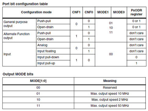
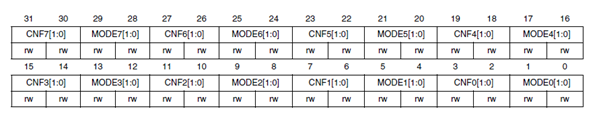
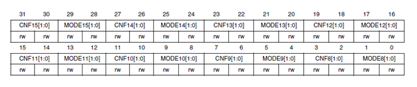
- CRL sets GPIOs from 0 – 7 while CRH sets from 8 – 15. All IO ports are 16 bit wide unlike common 8 bit micros like PIC or AVR.
CRL Register:
CRH Register:
- As can be seen from port configuration table, right after reset CRL and CRH both have a value of 0x44444444. This value means floating input mode.
- IDR registers are responsible for digital inputs while ODR registers are responsible for digital outputs. In both registers the upper 16 bits are always kept 0 because GPIOs are 16 bits wide while their representative registers are 32 bit wide. Thus only the lower 16 nibbles are of concern. The code writing convention will be 0x0000xxxx for IDRs and ODRs. The upper nibbles are reserved and thus set as zeroes.
- Just like CRL and CRH, IDR and ODR should be accessed as 32 words.
- CRL and CRH should be initialized first before using ODR or IDR registers of a GPIO port.
ODR Register:

IDR Register:
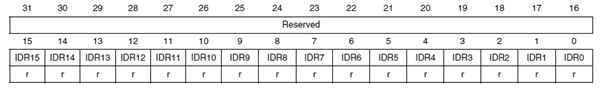
- Reset values of IDR and ODR are both zero. This ensures initial logic low state for ODR and float state for IDR.
- After each device reset, all peripheral clocks are disabled (except for the SRAM and FLITF). Before using a peripheral you have to enable its clock in the RCC_AHBENR, RCC_APB1ENR or RCC_APB2ENR register. These registers are important and should always be set before using an internal peripheral.
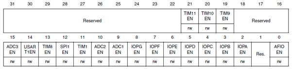
APB2 peripheral clock enable register (RCC_APB2ENR):
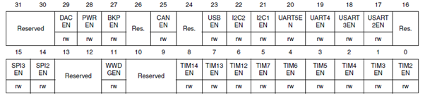
APB1 peripheral clock enable register (RCC_APB1ENR):
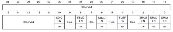
AHB peripheral clock enable register (RCC_AHBENR):
- The above registers should be set first before anything else.
MikroC for ARM has a built-in library for GPIO. Though such libraries are easy to get started with even without getting an insight of the internal registers, they are both space and execution time consuming things. Thus for simple works best is avoid them unless their use makes a big program easy to understand and deal with.
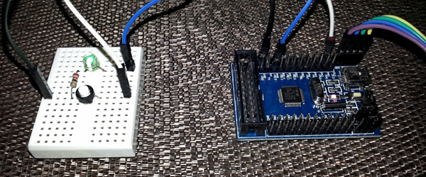
Example program
The program will just blink an LED connected to PB15 with an on time and off time of 200ms unless the button connected to PA0 is pressed. When the button is pressed the delay time is altered to 600ms instead of 200ms. 600ms delay is maintain until the button is released.
A STM32F108C8 micro embedded in a mini ARM development board from LC Technology was used in this demo.
Demo video clip: https://www.youtube.com/watch?v=X8jLZYZCCQw
Happy coding STM32.
Repository: https://github.com/sshahryiar/STM32-Tutorials
Author: Shawon M. Shahryiar
https://www.youtube.com/c/sshahryiar
|
|
Pingback: STM32 GPIO PORT ACCESSING | teknowtips
Pingback: Ссылки за 20-28 июня | MyLinks