XMega ADC
|
|
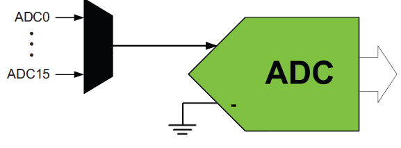
For users of advance MCUs like the XMega it is not necessary to tell what an analog-to-digital converter (ADC) is or what it does. I assume this is not the first family of microcontroller they are dealing with. Unlike the ADCs of other microcontroller the ADC of XMega devices is a highly complex tool. The level of complexity is so much that without understanding every bits-and-pieces of this piece of hardware a user won’t enjoy its absolute power. XMega ADC is also the most confusing hardware as it is not like other MCU ADCs. We will be dealing with ATXMega32A4U and it has only one ADC block, named ADCA but some other XMega devices like the XMega128A1 have more than one ADC block – ADCA and ADCB. By the way the XMega reference manual provides a long literature on the ADC and I’m not willing to state everything.
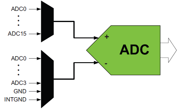
A quick view of the ADC block diagram shows most of the internal arrangement.
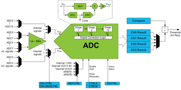
To begin with, there are some prerequisites. The very first thing is to realize the inputs of the ADC block (VINP and VINN) as like the two inputs of a regular op-amp. The ADC is differential in nature. Secondly there are several areas that need more than a few lines of “ATMEL” explanation and several assumptions. We can’t see the internal circuitry after all. Take things initially as if they are in black boxes and then slowly but systematically probe them until fully unveiled. This is somewhat a my-kind of learning technique. Thirdly a word of caution, an ADC channel doesn’t necessarily mean a physical ADC pin as in traditional MCUs. In the XMega32A4U there’s one physical ADC – ADCA comprising of four virtual channels that can be connected to a number of signal sources both internal and external (physical pins). Lastly we won’t be using 8 bit ADC conversions in our discussion anywhere as it is less precise and seldom used. However 8 bit conversions are faster than 12 bit ones.
Key Pros and Cons of XMega ADCs
Pros:
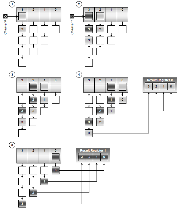
- Pipeline Architecture – Simply this feature allows one sample to be processed while another is being acquired. Here’s a conceptual view of how this stuff works.
- ADC’s power consumption can be controlled.
- High sampling rate (2Msps) and high resolution (12 bits).
- Several options for reference source.
- Conversion frequency can be set by pre-scaling peripheral clock.
- Signed/unsigned modes.
- Differential and single-end measurements.
- Front-end gain stage for differential modes, allowing amplification of small signals.
- ADC conversion can be triggered by events, timer interrupts, DMA requests and so on.
Cons:
- Unlike ordinary MCUs like the traditional AVR ATMega MCUs, ADC reference can’t be more than (VDD – 0.6) volts even if the reference source is externally connected.
- Calibration values are stored in signature row and these must be manually read and written to ADC. Again this feature is not common in the most popular microcontrollers.
- In terms of volts per ADC count and general perception, the ADC is not really 12bit but rather somewhat 11 bits or some less than 12 bit. More explanations later.
- In the unsigned single-ended mode of operation a small amount of positive offset is internally added to detect zero-cross. This is the reason why people will not get zero count at zero voltage. You will rather get a count of about 200 or so at zero voltage. This offset should be compensated in the software end and in the process the ADC is no long a 12 bit ADC for general purpose uses. Owing to this offset the maximum value of voltage the ADC can measure is also below the reference voltage. However a tiny amount of negative voltage can be detected in this mode.
Differential Mode
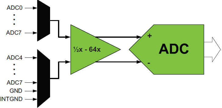
People who have dealt with instrumentations or analog electronics will certainly know what a differential amplifier is. Well basically it just amplifies/passes the difference in signal between its two input terminals. Simply Vout = m x (Vinp – Vinn), where m is the gain, Vinp is the positive input and Vinn is the negative input. In the XMega ADC block this differential mode is technically the same stuff. You have two ADC pins as inputs in differential mode and an optional gain stage. Typically use of differential mode is that for measuring current flowing through a shunt. However a few things are to be strictly followed:
- Only signed conversion is possible in differential mode. Thus the 12bit ADC count has a range from -2048 to 2047, centering at 0.
- All pins can be positive inputs but only a few specified and be negative inputs. Only ADC0 – ADC3 pins can be negative input pins in differential mode without gain while only ADC4 – ADC7 pins can be negative input pins in differential mode with gain. Other than these pins, negative inputs can also be tied with either the internal or pad (external) ground. When the negative input is tied to ground and an ADC input is used, the result is a signed single-ended ADC.
- Gain can be set according to need but the value of gain is a multiple of 2, ranging 0.5x to 64x.
- Additional gain stage adds additional propagation delays.
Single-Ended Mode
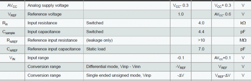
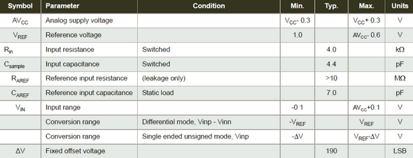
This is what people use mostly. Unlike the differential mode it has both signed and unsigned conversion mode of operation. The only difference between these modes is to what the negative terminal of the ADC block is connected to. Apparently single-ended mode seems to be the easiest and simple mode of operation but trust me this mode is where people get their head blown off. It took several days for me to understand this mode completely. Before going on further please note all of the figures, tables and formulae are taken from Atmel’s official docs and so nothing is based on imagination.
The key region of confusion of unsigned single-ended conversion mode is the ∆V offset. Its physical value is about 5% of the reference and so if the reference is 1.0V then its value is 0.05V. Remember what I said about differential amp earlier? If so then check the block diagram shown below.
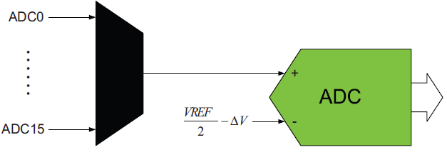
The negative input is connected to some sort of reference. This is the first piece of confusion and things get more complicated to realize when you go through the formula for unsigned single-ended ADC conversion, which is:
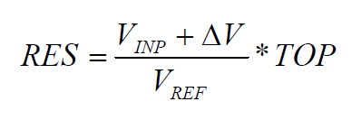
Note that the formula and the block diagram don’t technically agree with each other. Throughout all Atmel’s technical docs I found the same stuff over and over again with no elaborate explanation. However what I found during my research is that the formula is consistent. I didn’t find any answer to the missing VREF / 2 part. My first question was why it is connected to some sort of offset rather than zero. The answer is somewhat both easy and complicated. By having the ADC configured internally this way an XMega ADC pin connected to ground (0.0V) does not give 0 ADC count but about 200 ADC counts. I thought it was a hardware bug and that the ADC is not truly a 12 bits ADC but somewhat less than that. The more I researched the more I found it to be useful. If 0V in an ADC pin results about 200 counts then definitely a small negative voltage at that ADC pin will result 0 ADC count. According to Atmel this offset helps to detect zero-crossing or true 0V rather than something near to 0V like ±0.001. I found that the XMega ADC can, in fact, detect a tiny quantity of negative potential. Usually we don’t use this feature with common ADC uses but in certain precision instrumentations we need to know this and there this offset plays its part. If you check XMega datasheet then you’ll notice that ADC input voltage range spans from -0.1V to (AVCC + 0.1) V. Though this feature has its advantage in some certain areas it comes at a cost of reduced top range which about 95% of the reference source’s value. If, for example, the internal 1.0V reference is used then the ADC can measure voltages ranging from about -0.05V to about 0.95V. Thus it is still measuring a 1.0V span with 12 bits precision though apparently it may not look like that at first experience. Fortunately MikroC PRO for AVR compiler’s ADC library is based on this mode of operation and so be aware not to curse yourself.
In the signed single-ended mode VINN is connected to ground and it is quite a simple story. In the signed mode the result of an ADC conversion is always 11bits. The MSB is used for sign. However you cannot apply negative voltage to an ADC pin with respect to ground under any circumstances except what your device’s datasheet states. You’ll get 0 – 2047 counts for 0V – VREF range.
My Experiences and Findings
I found a number of stuffs that I feel needs to be shared apart from whatever I already stated. In my experience the internal 1.0V source is not good enough as a reference source for ADC because it needs a lot of caution and even some people claim that Atmel said that this source is technically too low for an ADC reference. I did try to use it but I found it to be too sensitive to noise. At this point Atmel recommended to shut down all operations of the MCU or go to sleep mode during capturing an ADC sample. This may not be always possible. There are other options for reference source but I found out that the best one is the VCC / 1.6 reference source. With 3.3V VCC, it is about 2.06V. However a lot of care is needed to ensure a good stable VCC. Since a MCU is a digital device there will be switching noise across the power lines and to reduce them we need to follow basic EMI and PCB routing principles. AVCC pins should be connected to VCC via a ferrite bead and a 100nF capacitor. All other VDD pins should have 100nF capacitors connected between them and ground. Another good solution for ADC reference source is to use external reference sources like TL431 and similar.
Since the ADC is of 12 bit resolution and the reference source is less than 3.3V, the ADC block will tend to pick up noises and tiny fluctuations. The ADC count may vary as much as 60 counts. To avoid these we need to follow recommendations from Atmel and apply some basic tips. ADC values should be averaged in the software end. If possible ADC pins should be buffered and filtered externally with proper low pass LC filter. XMega ADCs offer high impedance and low impedance modes along with other options to control ADC power consumption. Temperature compensation can also be used to improve ADC accuracy. If properly configured a lot of problem is dealt with easily.
A must do process is to get rid of any offset before using the ADC for actual measurements. This can be done in two ways. First is to ground any ADC pin that will be used for taking measurements later, get the ADC offset with that pin and then use it normally as it was intended. This offset is common and so it is not needed to measure the offset for all ADC pins. The other method is to dedicate an ADC pin to ground and it will never be disconnected from ground. This will measure the offset only. In terms of pin count this method is expensive but it is the most hassle-free process. Actually I prefer this method.
In most applications the signed single-ended mode is the best to use. The other is to use differential mode without gain and negative input tied to ground. When using differential mode with gain be aware of noise because noise also gets amplified along with signal. Be sure to select proper ADC sampling frequency. For general purpose uses something from 60 – 150kHz as sampling rate is good enough. Please also note that Atmel recommends that the user must access and load factory calibration bytes for proper operation of the ADC. Frankly speaking in all of the XMega MCUs I have at my disposal, I found that the calibration bytes for ADC in them are 0x00. I don’t find it necessary to load these meaningless values but I still used them in my coding to go by Atmel’s recommended way.
Before using a ADC pin make sure that it is a floating pin. If you have read my previous post on XMega I/O ports then you must know how to do it.
Code Examples
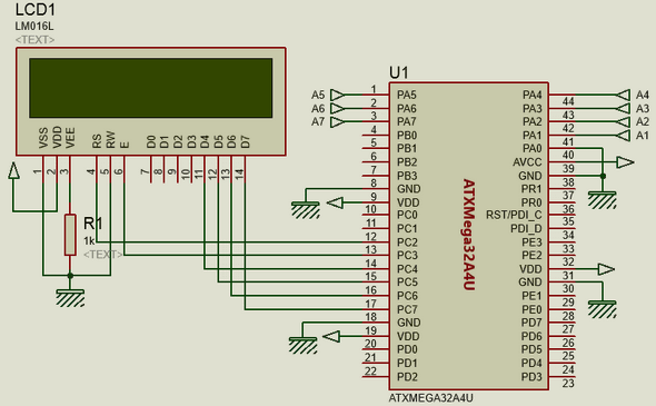
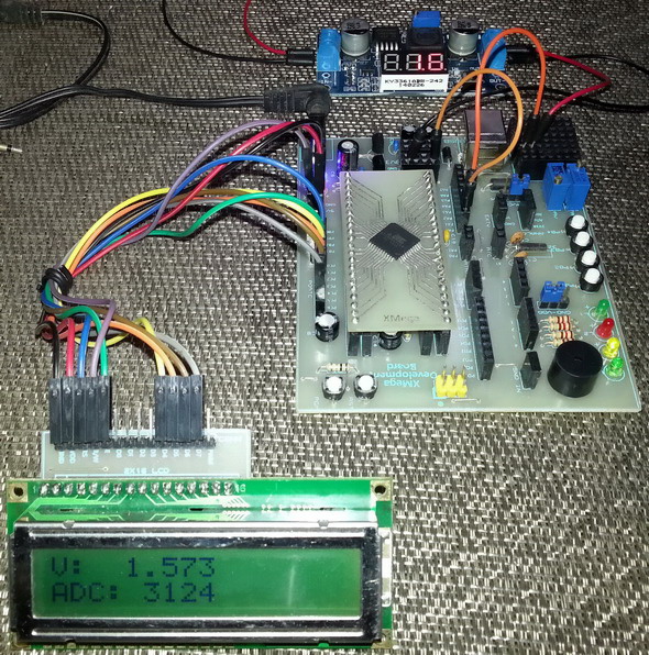
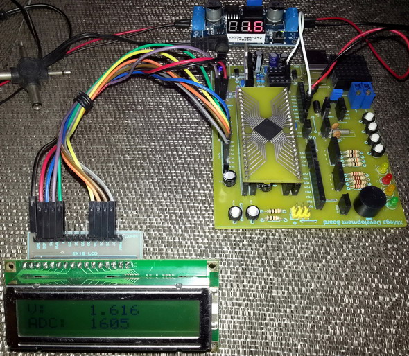
Just as before, I added a header file for ADC along with the header files for clock and I/O ports. This will greatly reduce coding time and efforts. In my coding I followed a systematic procedure to configure the MCU. I recommend following this method. First configure the XMega clock, then I/O port pins and finally the ADC itself. In all of my example codes the XMega CPU is configured to run at 8MHz clock speed and only PORTA pins are used for ADC inputs. A LCD with the help of MikroC’s library provided a mean to see ADC data during tests.. As always using MikroC’s libraries are fun, fast and easy but they come at the cost of reduced customizations and relatively larger code sizes. Shown below is the basic setup:
XMega ADC with MikroC’s Library
#include <io.h>
#include <clock.h>
sbit LCD_RS at PORTC_OUT.B2;
sbit LCD_EN at PORTC_OUT.B3;
sbit LCD_D4 at PORTC_OUT.B4;
sbit LCD_D5 at PORTC_OUT.B5;
sbit LCD_D6 at PORTC_OUT.B6;
sbit LCD_D7 at PORTC_OUT.B7;
sbit LCD_RS_Direction at PORTC_DIR.B2;
sbit LCD_EN_Direction at PORTC_DIR.B3;
sbit LCD_D4_Direction at PORTC_DIR.B4;
sbit LCD_D5_Direction at PORTC_DIR.B5;
sbit LCD_D6_Direction at PORTC_DIR.B6;
sbit LCD_D7_Direction at PORTC_DIR.B7;
void setup();
signed int adc_avg(unsigned char no_of_samples, unsigned char channel);
void lcd_print(unsigned char x_pos, unsigned char y_pos, signed int value, unsigned char cnt_volt);
float map(float v, float x_min, float x_max, float y_min, float y_max);
void main()
{
signed int adc = 0;
signed int offset = 0;
float v = 0;
setup();
offset = adc_avg(100, 0);
lcd_out(1, 1, "V:");
lcd_out(2, 1, "ADC:");
while(1)
{
adc = adc_avg(50, 1);
v = map(adc, offset, 4095.0, 0, 1959.375);
lcd_print(4, 1, v, 0);
lcd_print(5, 2, adc, 1);
delay_ms(600);
};
}
void setup()
{
OSC_CTRL |= OSC_RC32KEN_bm;
while(!(OSC_STATUS & OSC_RC32KRDY_bm));
OSC_CTRL |= OSC_RC32MEN_bm;
CPU_CCP = CCP_IOREG_gc;
CLK_PSCTRL = ((CLK_PSCTRL & (~(CLK_PSADIV_gm | CLK_PSBCDIV1_bm | CLK_PSBCDIV0_bm)))
| CLK_PSADIV_1_gc | CLK_PSBCDIV_2_2_gc);
OSC_DFLLCTRL = ((OSC_DFLLCTRL & (~(OSC_RC32MCREF_gm | OSC_RC2MCREF_bm))) |
OSC_RC32MCREF_RC32K_gc);
DFLLRC32M_CTRL |= DFLL_ENABLE_bm;
while(!(OSC_STATUS & OSC_RC32MRDY_bm));
CPU_CCP = CCP_IOREG_gc;
CLK_CTRL = ((CLK_CTRL & (~CLK_SCLKSEL_gm)) | CLK_SCLKSEL_RC32M_gc);
OSC_CTRL &= (~(OSC_RC2MEN_bm | OSC_XOSCEN_bm | OSC_PLLEN_bm));
PORTCFG_CLKEVOUT = 0x00;
PORTD_OUT = 0x00;
PORTD_DIR = 0x02;
PORTD_PIN0CTRL = (PORT_OPC_BUSKEEPER_gc | PORT_ISC_BOTHEDGES_gc);
PORTD_PIN1CTRL = (PORT_OPC_TOTEM_gc | PORT_ISC_BOTHEDGES_gc);
ADCA_Init_Advanced(_ADC_12bit, _ADC_INTERNAL_REF_VCC);
Lcd_Init();
Lcd_Cmd(_LCD_CLEAR);
Lcd_Cmd(_LCD_CURSOR_OFF);
}
signed int adc_avg(unsigned char no_of_samples, unsigned char channel)
{
signed long avg = 0;
unsigned char samples = no_of_samples;
while(samples > 0)
{
avg += ADCA_Get_Sample(channel);
samples--;
}
avg /= no_of_samples;
return avg;
}
void lcd_print(unsigned char x_pos, unsigned char y_pos, signed int value, unsigned char cnt_volt)
{
unsigned char tmp = 0;
if(value > 0)
{
lcd_out(y_pos, x_pos, " ");
}
else
{
lcd_out(y_pos, x_pos, "-");
value *= -1;
}
tmp = (value / 1000);
lcd_chr_cp(tmp + 48);
switch(cnt_volt)
{
case 1:
{
break;
}
default:
{
lcd_chr_cp(46);
break;
}
}
tmp = ((value / 100) % 10);
lcd_chr_cp((tmp + 48));
tmp = ((value / 10) % 10);
lcd_chr_cp((tmp + 48));
tmp = (value % 10);
       lcd_chr_cp((tmp + 48));
}
float map(float v, float x_min, float x_max, float y_min, float y_max)
{
float m = 0.0;
m = ((y_max - y_min)/(x_max - x_min));
return (y_min + (m * (v - x_min)));
}
Video Link: https://www.youtube.com/watch?v=xB7MZZ9FFw4
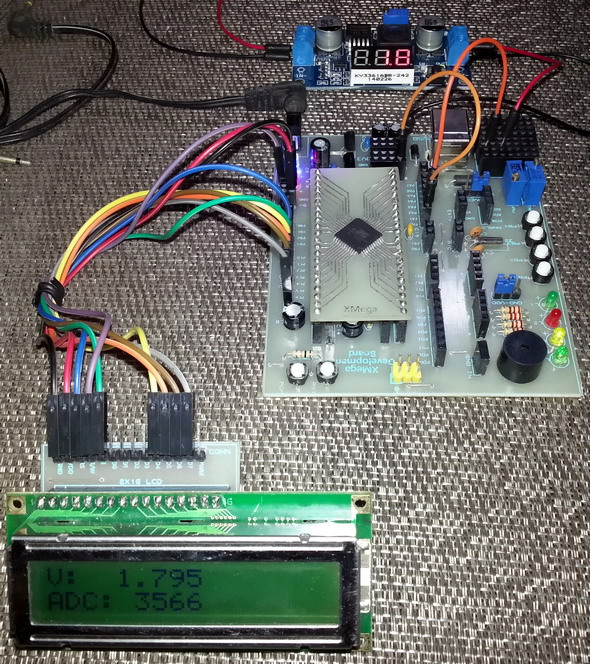
XMega ADC Unsigned Single-Ended
#include <io.h>
#include <adc.h>
#include <clock.h>
sbit LCD_RS at PORTC_OUT.B2;
sbit LCD_EN at PORTC_OUT.B3;
sbit LCD_D4 at PORTC_OUT.B4;
sbit LCD_D5 at PORTC_OUT.B5;
sbit LCD_D6 at PORTC_OUT.B6;
sbit LCD_D7 at PORTC_OUT.B7;
sbit LCD_RS_Direction at PORTC_DIR.B2;
sbit LCD_EN_Direction at PORTC_DIR.B3;
sbit LCD_D4_Direction at PORTC_DIR.B4;
sbit LCD_D5_Direction at PORTC_DIR.B5;
sbit LCD_D6_Direction at PORTC_DIR.B6;
sbit LCD_D7_Direction at PORTC_DIR.B7;
signed int offset = 0;
void clock_setup();
void io_setup();
void adc_setup();
void setup();
signed int ADCA_read_ext_pins(unsigned char pin);
signed int adc_avg(unsigned char no_of_samples, unsigned char pin);
void lcd_print(unsigned char x_pos, unsigned char y_pos, signed int value, unsigned char cnt_volt);
float map(float v, float x_min, float x_max, float y_min, float y_max);
void main()
{
signed int adc = 0;
float v = 0;
setup();
lcd_out(1, 1, "V:");
lcd_out(2, 1, "ADC:");
while(1)
{
adc = adc_avg(25, ADC_CH_MUXPOS_PIN1_gc);
v = map(adc, offset, 4095.0, 0, 1959.375);
lcd_print(4, 1, v, 0);
lcd_print(5, 2, adc, 1);
delay_ms(600);
};
}
void clock_setup()
{
OSC_CTRL |= OSC_RC32KEN_bm;
while(!(OSC_STATUS & OSC_RC32KRDY_bm));
OSC_CTRL |= OSC_RC32MEN_bm;
CPU_CCP = CCP_IOREG_gc;
CLK_PSCTRL = ((CLK_PSCTRL & (~(CLK_PSADIV_gm | CLK_PSBCDIV1_bm | CLK_PSBCDIV0_bm)))
| CLK_PSADIV_1_gc | CLK_PSBCDIV_2_2_gc);
OSC_DFLLCTRL = ((OSC_DFLLCTRL & (~(OSC_RC32MCREF_gm | OSC_RC2MCREF_bm))) |
OSC_RC32MCREF_RC32K_gc);
DFLLRC32M_CTRL |= DFLL_ENABLE_bm;
while(!(OSC_STATUS & OSC_RC32MRDY_bm));
CPU_CCP = CCP_IOREG_gc;
CLK_CTRL = ((CLK_CTRL & (~CLK_SCLKSEL_gm)) | CLK_SCLKSEL_RC32M_gc);
OSC_CTRL &= (~(OSC_RC2MEN_bm | OSC_XOSCEN_bm | OSC_PLLEN_bm));
PORTCFG_CLKEVOUT = 0x00;
}
void io_setup()
{
PORTA_OUT = 0x00;
PORTA_DIR = 0x00;
PORTCFG_MPCMASK = 0xFF;
PORTA_PIN0CTRL = (PORT_OPC_TOTEM_gc | PORT_ISC_BOTHEDGES_gc);
PORTA_INTCTRL = 0x00;
PORTA_INT0MASK = 0x00;
PORTA_INT1MASK = 0x00;
}
void adc_setup()
{
unsigned char samples = 16;
ADCA_CAL = (0x0FFF & ((PROD_SIGNATURES_ADCACAL1 << 8) | PROD_SIGNATURES_ADCACAL0));
ADCA_CTRLB = ((1 << ADC_IMPMODE_bp) | ADC_CURRLIMIT_NO_gc | (0 << ADC_CONMODE_bp) | ADC_RESOLUTION_12BIT_gc);
ADCA_PRESCALER = ADC_PRESCALER_DIV64_gc;
ADCA_REFCTRL = (ADC_REFSEL_VCC_gc | (0 << ADC_TEMPREF_bp) | (0 << ADC_BANDGAP_bp));
ADCA_CH0_CTRL = ((0 << ADC_CH_START_bp) | ADC_CH_INPUTMODE_SINGLEENDED_gc);
ADCA_CH0_MUXCTRL = ADC_CH_MUXPOS_PIN0_gc;
ADCA_CTRLA |= ADC_ENABLE_bm;
delay_ms(4);
while(samples > 0)
{
ADCA_CH0_CTRL |= (1 << ADC_CH_START_bp);
while(!(ADCA_CH0_INTFLAGS & ADC_CH_CHIF_bm));
ADCA_CH0_INTFLAGS = ADC_CH_CHIF_bm;
offset += ADCA_CH0RES;
samples--;
}
ADCA_CTRLA &= ~ADC_ENABLE_bm;
offset >>= 4;
ADCA_CMP = 0x0000;
ADCA_CH0_CTRL = ((0 << ADC_CH_START_bp) | ADC_CH_GAIN_1X_gc | ADC_CH_INPUTMODE_SINGLEENDED_gc);
ADCA_CH0_MUXCTRL = ADC_CH_MUXPOS_PIN1_gc;
ADCA_EVCTRL = (ADC_SWEEP_0_gc | ADC_EVACT_NONE_gc);
ADCA_CH0_INTCTRL = (ADC_CH_INTMODE_COMPLETE_gc | ADC_CH_INTLVL_OFF_gc);
ADCA_CH1_INTCTRL = ADC_CH_INTLVL_OFF_gc;
ADCA_CH2_INTCTRL = ADC_CH_INTLVL_OFF_gc;
ADCA_CH3_INTCTRL = ADC_CH_INTLVL_OFF_gc;
ADCA_CTRLB |= ADC_FREERUN_bm;
ADCA_CTRLA |= ADC_ENABLE_bm;
delay_ms(9);
}
void setup()
{
clock_setup();
io_setup();
adc_setup();
Lcd_Init();
Lcd_Cmd(_LCD_CLEAR);
Lcd_Cmd(_LCD_CURSOR_OFF);
}
signed int ADCA_read_ext_pins(unsigned char pin)
{
signed int val = 0;
ADCA_CH0_MUXCTRL = pin;
while(!(ADCA_CH0_INTFLAGS & ADC_CH_CHIF_bm));
ADCA_CH0_INTFLAGS = ADC_CH_CHIF_bm;
val = ADCA_CH0_RES;
return val;
}
signed int adc_avg(unsigned char no_of_samples, unsigned char pin)
{
signed long avg = 0;
unsigned char samples = no_of_samples;
while(samples > 0)
{
avg += ADCA_read_ext_pins(pin);
samples--;
}
avg /= no_of_samples;
return avg;
}
void lcd_print(unsigned char x_pos, unsigned char y_pos, signed int value, unsigned char cnt_volt)
{
unsigned char tmp = 0;
if(value > 0)
{
lcd_out(y_pos, x_pos, " ");
}
else
{
lcd_out(y_pos, x_pos, "-");
value *= -1;
}
tmp = (value / 1000);
lcd_chr_cp(tmp + 48);
switch(cnt_volt)
{
case 1:
{
break;
}
default:
{
lcd_chr_cp(46);
break;
}
}
tmp = ((value / 100) % 10);
lcd_chr_cp((tmp + 48));
tmp = ((value / 10) % 10);
lcd_chr_cp((tmp + 48));
tmp = (value % 10);
lcd_chr_cp((tmp + 48));
}
float map(float v, float x_min, float x_max, float y_min, float y_max)
{
float m = 0.0;
m = ((y_max - y_min)/(x_max - x_min));
return (y_min + (m * (v - x_min)));
}
Video Link: https://www.youtube.com/watch?v=4v042tw5IQY
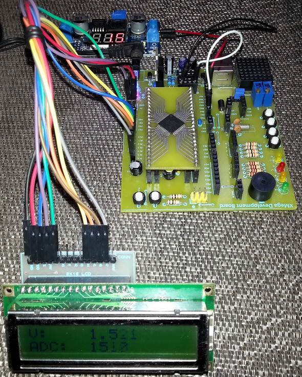
XMega ADC Signed Single-Ended
#include <io.h>
#include <adc.h>
#include <clock.h>
sbit LCD_RS at PORTC_OUT.B2;
sbit LCD_EN at PORTC_OUT.B3;
sbit LCD_D4 at PORTC_OUT.B4;
sbit LCD_D5 at PORTC_OUT.B5;
sbit LCD_D6 at PORTC_OUT.B6;
sbit LCD_D7 at PORTC_OUT.B7;
sbit LCD_RS_Direction at PORTC_DIR.B2;
sbit LCD_EN_Direction at PORTC_DIR.B3;
sbit LCD_D4_Direction at PORTC_DIR.B4;
sbit LCD_D5_Direction at PORTC_DIR.B5;
sbit LCD_D6_Direction at PORTC_DIR.B6;
sbit LCD_D7_Direction at PORTC_DIR.B7;
signed int offset = 0;
void clock_setup();
void io_setup();
void adc_setup();
void setup();
signed int ADCA_read_ext_pins(unsigned char pin);
signed int adc_avg(unsigned char no_of_samples, unsigned char pin);
void lcd_print(unsigned char x_pos, unsigned char y_pos, signed int value, unsigned char cnt_volt);
void main()
{
signed int adc = 0;
float v = 0;
setup();
lcd_out(1, 1, "V:");
lcd_out(2, 1, "ADC:");
while(1)
{
adc = adc_avg(25, ADC_CH_MUXPOS_PIN7_gc);
v = ((adc * 2062.5) / 2047);
lcd_print(6, 1, v, 0);
lcd_print(6, 2, adc, 1);
delay_ms(600);
};
}
void clock_setup()
{
OSC_CTRL |= OSC_RC32KEN_bm;
while(!(OSC_STATUS & OSC_RC32KRDY_bm));
OSC_CTRL |= OSC_RC32MEN_bm;
CPU_CCP = CCP_IOREG_gc;
CLK_PSCTRL = ((CLK_PSCTRL & (~(CLK_PSADIV_gm | CLK_PSBCDIV1_bm | CLK_PSBCDIV0_bm)))
| CLK_PSADIV_1_gc | CLK_PSBCDIV_2_2_gc);
OSC_DFLLCTRL = ((OSC_DFLLCTRL & (~(OSC_RC32MCREF_gm | OSC_RC2MCREF_bm))) |
OSC_RC32MCREF_RC32K_gc);
DFLLRC32M_CTRL |= DFLL_ENABLE_bm;
while(!(OSC_STATUS & OSC_RC32MRDY_bm));
CPU_CCP = CCP_IOREG_gc;
CLK_CTRL = ((CLK_CTRL & (~CLK_SCLKSEL_gm)) | CLK_SCLKSEL_RC32M_gc);
OSC_CTRL &= (~(OSC_RC2MEN_bm | OSC_XOSCEN_bm | OSC_PLLEN_bm));
PORTCFG_CLKEVOUT = 0x00;
}
void io_setup()
{
PORTA_OUT = 0x00;
PORTA_DIR = 0x00;
PORTCFG_MPCMASK = 0xFF;
PORTA_PIN0CTRL = (PORT_OPC_TOTEM_gc | PORT_ISC_BOTHEDGES_gc);
PORTA_INTCTRL = 0x00;
PORTA_INT0MASK = 0x00;
PORTA_INT1MASK = 0x00;
}
void adc_setup()
{
unsigned char samples = 16;
ADCA_CAL = (0x0FFF & ((PROD_SIGNATURES_ADCACAL1 << 8) | PROD_SIGNATURES_ADCACAL0));
ADCA_CTRLB = ((0 << ADC_IMPMODE_bp) | ADC_CURRLIMIT_NO_gc | (1 << ADC_CONMODE_bp) | ADC_RESOLUTION_12BIT_gc);
ADCA_PRESCALER = ADC_PRESCALER_DIV64_gc;
ADCA_REFCTRL = (ADC_REFSEL_VCC_gc | (0 << ADC_TEMPREF_bp) | (0 << ADC_BANDGAP_bp));
ADCA_CH0_CTRL = ((0 << ADC_CH_START_bp) | ADC_CH_GAIN_1X_gc | ADC_CH_INPUTMODE_DIFF_gc);
ADCA_CH0_MUXCTRL = (ADC_CH_MUXPOS_PIN0_gc | ADC_CH_MUXNEG_PIN0_gc);
ADCA_CTRLA |= ADC_ENABLE_bm;
delay_ms(4);
while(samples > 0)
{
ADCA_CH0_CTRL |= (1 << ADC_CH_START_bp);
while(!(ADCA_CH0_INTFLAGS & ADC_CH_CHIF_bm));
ADCA_CH0_INTFLAGS = ADC_CH_CHIF_bm;
offset += ADCA_CH0RES;
samples--;
}
ADCA_CTRLA &= ~ADC_ENABLE_bm;
offset >>= 4;
ADCA_CMP = 0x0000;
ADCA_CH0_CTRL = ((0 << ADC_CH_START_bp) | ADC_CH_GAIN_1X_gc | ADC_CH_INPUTMODE_SINGLEENDED_gc);
ADCA_CH0_MUXCTRL = ADC_CH_MUXPOS_PIN7_gc;
ADCA_EVCTRL = (ADC_SWEEP_0_gc | ADC_EVACT_NONE_gc);
ADCA_CH0_INTCTRL = (ADC_CH_INTMODE_COMPLETE_gc | ADC_CH_INTLVL_OFF_gc);
ADCA_CH1_INTCTRL = ADC_CH_INTLVL_OFF_gc;
ADCA_CH2_INTCTRL = ADC_CH_INTLVL_OFF_gc;
ADCA_CH3_INTCTRL = ADC_CH_INTLVL_OFF_gc;
ADCA_CTRLB |= ADC_FREERUN_bm;
ADCA_CTRLA |= ADC_ENABLE_bm;
delay_ms(9);
}
void setup()
{
clock_setup();
io_setup();
adc_setup();
Lcd_Init();
Lcd_Cmd(_LCD_CLEAR);
Lcd_Cmd(_LCD_CURSOR_OFF);
}
signed int ADCA_read_ext_pins(unsigned char pin)
{
signed int val = 0;
ADCA_CH0_MUXCTRL = pin;
while (!(ADCA_CH0_INTFLAGS & ADC_CH_CHIF_bm));
ADCA_CH0_INTFLAGS = ADC_CH_CHIF_bm;
val = ADCA_CH0_RES;
if (val > offset)
{
val -= offset;
}
else
{
val = 0;
}
return val;
}
signed int adc_avg(unsigned char no_of_samples, unsigned char pin)
{
signed long avg = 0;
unsigned char samples = no_of_samples;
while(samples > 0)
{
avg += ADCA_read_ext_pins(pin);
samples--;
}
avg /= no_of_samples;
return avg;
}
void lcd_print(unsigned char x_pos, unsigned char y_pos, signed int value, unsigned char cnt_volt)
{
unsigned char tmp = 0;
if(value > 0)
{
lcd_out(y_pos, x_pos, " ");
}
else
{
lcd_out(y_pos, x_pos, "-");
value *= -1;
}
tmp = (value / 1000);
lcd_chr_cp(tmp + 48);
switch(cnt_volt)
{
case 1:
{
break;
}
default:
{
lcd_chr_cp(46);
break;
}
}
tmp = ((value / 100) % 10);
lcd_chr_cp((tmp + 48));
tmp = ((value / 10) % 10);
lcd_chr_cp((tmp + 48));
tmp = (value % 10);
lcd_chr_cp((tmp + 48));
}

Video Link: https://www.youtube.com/watch?v=xC43v_35zRA
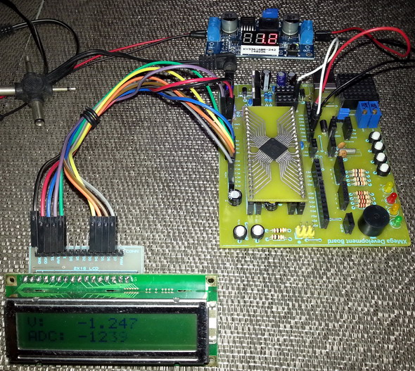
XMega ADC Differential Conversion Mode
#include <io.h>
#include <adc.h>
#include <clock.h>
sbit LCD_RS at PORTC_OUT.B2;
sbit LCD_EN at PORTC_OUT.B3;
sbit LCD_D4 at PORTC_OUT.B4;
sbit LCD_D5 at PORTC_OUT.B5;
sbit LCD_D6 at PORTC_OUT.B6;
sbit LCD_D7 at PORTC_OUT.B7;
sbit LCD_RS_Direction at PORTC_DIR.B2;
sbit LCD_EN_Direction at PORTC_DIR.B3;
sbit LCD_D4_Direction at PORTC_DIR.B4;
sbit LCD_D5_Direction at PORTC_DIR.B5;
sbit LCD_D6_Direction at PORTC_DIR.B6;
sbit LCD_D7_Direction at PORTC_DIR.B7;
signed int offset = 0;
void clock_setup();
void io_setup();
void adc_setup();
void setup();
signed int ADCA_read_ext_pins(unsigned char pos_pin, unsigned char neg_pin);
signed int adc_avg(unsigned char no_of_samples, unsigned char pos_pin, unsigned char neg_pin);
void lcd_print(unsigned char x_pos, unsigned char y_pos, signed int value, unsigned char cnt_volt);
void main()
{
signed int adc = 0;
float v = 0;
setup();
lcd_out(1, 1, "V:");
lcd_out(2, 1, "ADC:");
while(1)
{
adc = adc_avg(20, ADC_CH_MUXPOS_PIN1_gc, ADC_CH_MUXNEG_PIN2_gc);
v = ((adc * 2062.5) / 2048);
lcd_print(6, 1, v, 0);
lcd_print(6, 2, adc, 1);
delay_ms(600);
};
}
void clock_setup()
{
OSC_CTRL |= OSC_RC32KEN_bm;
while(!(OSC_STATUS & OSC_RC32KRDY_bm));
OSC_CTRL |= OSC_RC32MEN_bm;
CPU_CCP = CCP_IOREG_gc;
CLK_PSCTRL = ((CLK_PSCTRL & (~(CLK_PSADIV_gm | CLK_PSBCDIV1_bm | CLK_PSBCDIV0_bm)))
| CLK_PSADIV_1_gc | CLK_PSBCDIV_2_2_gc);
OSC_DFLLCTRL = ((OSC_DFLLCTRL & (~(OSC_RC32MCREF_gm | OSC_RC2MCREF_bm))) |
OSC_RC32MCREF_RC32K_gc);
DFLLRC32M_CTRL |= DFLL_ENABLE_bm;
while(!(OSC_STATUS & OSC_RC32MRDY_bm));
CPU_CCP = CCP_IOREG_gc;
CLK_CTRL = ((CLK_CTRL & (~CLK_SCLKSEL_gm)) | CLK_SCLKSEL_RC32M_gc);
OSC_CTRL &= (~(OSC_RC2MEN_bm | OSC_XOSCEN_bm | OSC_PLLEN_bm));
PORTCFG_CLKEVOUT = 0x00;
}
void io_setup()
{
PORTA_OUT = 0x00;
PORTA_DIR = 0x00;
PORTCFG_MPCMASK = 0xFF;
PORTA_PIN0CTRL = (PORT_OPC_TOTEM_gc | PORT_ISC_BOTHEDGES_gc);
PORTA_INTCTRL = 0x00;
PORTA_INT0MASK = 0x00;
PORTA_INT1MASK = 0x00;
}
void adc_setup()
{
unsigned char samples = 16;
ADCA_CAL = (0x0FFF & ((PROD_SIGNATURES_ADCACAL1 << 8) | PROD_SIGNATURES_ADCACAL0));
ADCA_CTRLB = ((1 << ADC_IMPMODE_bp) | ADC_CURRLIMIT_NO_gc | (1 << ADC_CONMODE_bp) | ADC_RESOLUTION_12BIT_gc);
ADCA_PRESCALER = ADC_PRESCALER_DIV64_gc;
ADCA_REFCTRL = (ADC_REFSEL_VCC_gc | (0 << ADC_TEMPREF_bp) | (0 << ADC_BANDGAP_bp));
ADCA_CH0_CTRL = ((0 << ADC_CH_START_bp) | ADC_CH_GAIN_1X_gc | ADC_CH_INPUTMODE_DIFF_gc);
ADCA_CH0_MUXCTRL = (ADC_CH_MUXPOS_PIN0_gc | ADC_CH_MUXNEG_PIN0_gc);
ADCA_CTRLA |= ADC_ENABLE_bm;
delay_ms(4);
while(samples > 0)
{
ADCA_CH0_CTRL |= (1 << ADC_CH_START_bp);
while(!(ADCA_CH0_INTFLAGS & ADC_CH_CHIF_bm));
ADCA_CH0_INTFLAGS = ADC_CH_CHIF_bm;
offset += ADCA_CH0RES;
samples--;
}
ADCA_CTRLA &= ~ADC_ENABLE_bm;
offset >>= 4;
ADCA_CH0_CTRL = ((0 << ADC_CH_START_bp) | ADC_CH_GAIN_1X_gc | ADC_CH_INPUTMODE_DIFF_gc);
ADCA_CH0_MUXCTRL = (ADC_CH_MUXPOS_PIN1_gc | ADC_CH_MUXNEG_PIN2_gc);
ADCA_EVCTRL = (ADC_SWEEP_0_gc | ADC_EVACT_NONE_gc);
ADCA_CH0_INTCTRL = (ADC_CH_INTMODE_COMPLETE_gc | ADC_CH_INTLVL_OFF_gc);
ADCA_CH1_INTCTRL = ADC_CH_INTLVL_OFF_gc;
ADCA_CH2_INTCTRL = ADC_CH_INTLVL_OFF_gc;
ADCA_CH3_INTCTRL = ADC_CH_INTLVL_OFF_gc;
ADCA_CTRLB |= ADC_FREERUN_bm;
ADCA_CTRLA |= ADC_ENABLE_bm;
delay_ms(9);
}
void setup()
{
clock_setup();
io_setup();
adc_setup();
Lcd_Init();
Lcd_Cmd(_LCD_CLEAR);
Lcd_Cmd(_LCD_CURSOR_OFF);
}
signed int ADCA_read_ext_pins(unsigned char pos_pin, unsigned char neg_pin)
{
signed int val = 0;
ADCA_CH0_MUXCTRL = (pos_pin | neg_pin);
while (!(ADCA_CH0_INTFLAGS & ADC_CH_CHIF_bm));
ADCA_CH0_INTFLAGS = ADC_CH_CHIF_bm;
val = ADCA_CH0_RES;
val -= offset;
return val;
}
signed int adc_avg(unsigned char no_of_samples, unsigned char pos_pin, unsigned char neg_pin)
{
signed long avg = 0;
unsigned char samples = no_of_samples;
while(samples > 0)
{
avg += ADCA_read_ext_pins(pos_pin, neg_pin);
samples--;
}
avg /= no_of_samples;
return avg;
}
void lcd_print(unsigned char x_pos, unsigned char y_pos, signed int value, unsigned char cnt_volt)
{
unsigned char tmp = 0;
if(value > 0)
{
lcd_out(y_pos, x_pos, " ");
}
else
{
lcd_out(y_pos, x_pos, "-");
value *= -1;
}
tmp = (value / 1000);
lcd_chr_cp(tmp + 48);
switch(cnt_volt)
{
case 1:
{
break;
}
default:
{
lcd_chr_cp(46);
break;
}
}
tmp = ((value / 100) % 10);
lcd_chr_cp((tmp + 48));
tmp = ((value / 10) % 10);
lcd_chr_cp((tmp + 48));
tmp = (value % 10);
lcd_chr_cp((tmp + 48));
}
Video Link: https://www.youtube.com/watch?v=eiordbwrI0s
As always it is not always possible to show everything of a sophisticated MCU like the XMega in such a short discussion and so I leave some things for the reader. I didn’t show the following things in this post:
- ADC + DMA use
- ADC + event system
- ADC’s temperature compensation functionality
- ADC sweeping
- How virtual channels work
- ADC’s compare functionality
- ADC interrupt
- Differential ADC with gain as it is similar to differential ADC mode.
I believe if you understood the basic of XMega ADC then these are not die-hard issues. ADC of such a MCU is really both robust and sophisticated. Manufacturers try to give literally everything that users imagine and there sophistication emerges. I recommend going through Atmel’s official docs, especially the reference manual as they will help a lot. To be honest, I read several blogs and even visited sites like AVR Freaks beside Atmel’s docs only to see that people are way too lazy to think beyond the boundaries of Atmel’s ASF. Though the ASF has made life easier, it is doesn’t help raw level coders like me in many ways.
Files: XMega ADC.
Happy coding.
Author: Shawon M. Shahryiar
https://www.facebook.com/groups/microarena/
https://www.facebook.com/MicroArena
+8801970046495 30.10.2014
|
|
Hi
That’s a nice tutorial you made out there, but here is my question:
You said that ATXmega32A4U has only single ADC block but the literature available from Atmel website
(now MICROCHIP) says that ATXmega16A4U/32A4U/64A4U/128A4U has two ADC blocks. I am confused about whats right or wrong but can you tell me.
Thank You
Could you refer where you read so? On page no. 48 of the datasheet (not the reference manual) it reads “One Analog to Digital Converter (ADC)”…. Only larger devices like the XMega128A1 have dual ADC blocks….
Very good, thank you.
You are welcomed…. 🙂
Thanks for sharing your thoughts on jam tangan original pria.
Regards
Pingback: XMega Analog Comparator | The Sun
Pingback: XMega Analog Comparator - Arduino collector blog