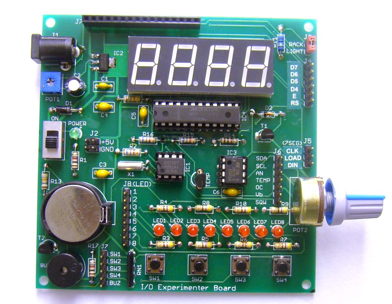
I/O Experimenter Board (PCB version)
|
|
Most embedded projects require the same common stuff, basically I/O devices such as switches, LEDs, LCD display, buzzer, etc. Connecting these things on a breadboard for prototyping every new project is time consuming and boring. Recently, I have designed a general purpose I/O experimenter board that will not only reduce the prototyping time for a new project but also free up plenty of space on the breadboard.

I/O Experimenter Board
This is actually a PCB version of my old project (A DIY I/O board for experimenters) with some additional features such as DS1307 RTC with battery back up and SPI seven segment LED display (4 digits). Here’s a list of the full features on board:
- On board +5V regulator IC (AMS1117 or equivalent).
- 16-pin female header for HD44780 based character LCD interface. Data (4-bit mode) and control pins are accessible through headers. A contrast adjustment potentiometer is available on the board. LCD backlight is turned ON and OFF using a 2-pin jumper)
- ON board MAX7219 provides 3-wire SPI interface to control a 4-digit seven segment LED display. The PCB is designed for any XX-5641AX series 0.56″ CC display module (4-digit), such as NFD-5461.
- IC Sockets for 24CXX EEPROM and a DS1307 RTC. I2C signal lines are accessible through headers.
- Socket for LM34 or any other analog temperature sensor that operates at +5V.
- A piezo buzzer with a transistor driver
- A potentiometer for ADC input signal
- A 2N2222 transistor open collector output for small load PWM demo
- 8 LEDs
- 4 Tact switches

Errors in silkscreen print are corrected by placing stickers on top (Left: Wrong, Right: Correct pin names)
The PCB size is approximately 3.94″ x 3.94″ (10cm x 10cm) and is manufactured from ITEADSTUDIO. I have got 10 PCBs of this I/O board and I am keeping 2 for myself and giving away rest of them for $7.50 per PCB including shipping within the USA. Email me at admin (at) embedded-lab (dot) com if you want to get the PCB and any other parts required to assemble the board. I will receive payment through Paypal only. I will send you my Paypal ID after I get email from you. I have also listed the PCB on Tindie. Here’s the link: https://tindie.com/rajbex/io-experimenter-board-pcb/

I/O Experimenter Board PCB
Here’s the list of parts that are required to assemble the board.

List of parts
I do have some extra parts to assemble the I/O board. I can provide a complete I/O Experimenter board kit (PCB+components) for $29.99. You will receive all the parts that are listed in the table above. The finished board will look like this. Note that the LCD display is not included in the kit. But you will receive a CR2032 battery, a MCP9701 temperature sensor, and a potentiometer knob as complimentary gifts with a kit.

Assembled I/O board

LCD display plugged in

Arduino prototyping is faster using the I/O board
Update (March 15, 2013)
This board has been corrected for the typo on the top silkscreen, and here is how the new board looks like. The access pins are also rearranged a little bit.

Revised I/O board

New list of items for the revised board
|
|
how can I get this pcb, being my country not found on your delivery …. if deign can I get a schematic and pcbnya? Thank you very much in advance
I am a student just learning electronics, I am interested in this pcb, but the position I was in Indonesia and I tried shopping there tindie.com not found for delivery to Indonesia. if pleased and hope your good, can I get a soft copy? I also do not mind if asked to reimburse the same as that sold in tindie.com pcb
Thank you very much
Hi Raj,
Any chance of publishing a schematic of the new design.
Thanks
Dear Sir,
I am a student from Sri Lanka. Will you be kind enough to give the Schematic and the PCB Layout of this board.
Thanks you
Raj…Just received your Experimenter Board – it’s a great job. A very nice, compact accessories board that greatly simplifies testing. And at a price that really shows up all the competition. I’m really looking forward to see how you top this unit. Thanks.
Just bought one of these from you, been looking for something like this for ages. Thank you
Pingback: I/O Experimenter Board (PCB version) | Make, Electronics projects, electronic Circuits, DIY projects, Microcontroller Projects - makeelectronic.com
Pingback: I/O Experimenter Board (PCB version) | electronics-projects.info
Excellent – At least of these is on the way to the UK…..
I love it! Your PCBs are just getting better and better.
Thanks, Dillon!