More on TI MSP430s
|
|
This post is a sequel of the first post on TI MSP430 micros here.
Low Power Modes (LPM)
From the smartwatches in our wrists to the vehicles we use for transportation, many modern electronic gadgets and gizmos are battery-powered. Some are even dependent on renewable energy sources like solar energy. In such devices, there is always an inherent energy crisis and so saving energy is a must in such designs for prolonged usage. At present there is hardly any microcontroller in the market that does not come equipped with energy-saving schemes or low power modes of operation. MSP430s were mainly designed for battery-backed instruments and it is no surprise that they come loaded with the some of the best possible energy-saving mechanisms.
There six modes of operation of which five are low power modes. These are as follows:
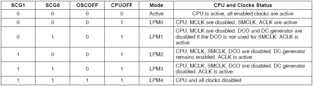
Of these six modes, three modes are mostly used – Active Mode (AM), LPM0 and LPM3. In Active Mode, the typical self-consumption of a MSP430 device is roughly about 300µA with nothing connected to it. In LPM0 the self-consumption is about a third of active mode while in LPM3, this consumption is just about 1µA. These figures tell us how much energy efficient MSP430s are.
Entering and exiting LPM is easy in terms of coding. However, the most common question that coders face with LPMs is how to get back to active mode or some other low power mode from a given low power mode. Well, it is pretty simple and it is accomplished with interrupts. It is up to coders to decide how to manage interrupts, clock sources and what do to after waking up from a LPM condition. Note that in LPMs, the CPU is disabled and so any task that requires CPU’s intervention is stalled. Since the CPU and some clocks are halted in LPMs, don’t even think that the tasks depending on them will be magically done. For instance, if a code has entered LPM3 and a timer is being driven with SMCLK, we should not expect it to tick because in LPM3, SMCLK is turned off. Organizing the code in a decent and well-planned manner is the secret behind successfully implementing LPMs.
Code Example
#include <msp430.h>
#include "delay.h"
void GPIO_graceInit(void);
void BCSplus_graceInit(void);
void System_graceInit(void);
void WDTplus_graceInit(void);
#pragma vector = PORT1_VECTOR
__interrupt void PORT1_ISR_HOOK(void)
{
LPM2_EXIT;
P1OUT |= BIT6;
P1IFG = 0x00;
}
void main(void)
{
unsigned char s = 0;
/* Stop watchdog timer from timing out during initial start-up. */
WDTCTL = WDTPW | WDTHOLD;
/* initialize Config for the MSP430 GPIO */
GPIO_graceInit();
/* initialize Config for the MSP430 2xx family clock systems (BCS) */
BCSplus_graceInit();
/* initialize Config for the MSP430 System Registers */
System_graceInit();
/* initialize Config for the MSP430 WDT+ */
WDTplus_graceInit();
while(1)
{
for(s = 0; s < 9; s++)
{
P1OUT ^= BIT0;
delay_ms(160);
}
P1OUT &= ~BIT6;
LPM2;
};
}
void GPIO_graceInit(void)
{
/* USER CODE START (section: GPIO_graceInit_prologue) */
/* User initialization code */
/* USER CODE END (section: GPIO_graceInit_prologue) */
/* Port 1 Output Register */
P1OUT = BIT3;
/* Port 1 Direction Register */
P1DIR = BIT0 | BIT6;
/* Port 1 Resistor Enable Register */
P1REN = BIT3;
/* Port 1 Interrupt Edge Select Register */
P1IES = BIT3;
/* Port 1 Interrupt Flag Register */
P1IFG = 0;
/* Port 1 Interrupt Enable Register */
P1IE = BIT3;
/* Port 2 Output Register */
P2OUT = 0;
/* Port 2 Port Select Register */
P2SEL &= ~(BIT6 | BIT7);
/* Port 2 Direction Register */
P2DIR = 0;
/* Port 2 Interrupt Edge Select Register */
P2IES = 0;
/* Port 2 Interrupt Flag Register */
P2IFG = 0;
/* USER CODE START (section: GPIO_graceInit_epilogue) */
/* User code */
/* USER CODE END (section: GPIO_graceInit_epilogue) */
}
void BCSplus_graceInit(void)
{
/* USER CODE START (section: BCSplus_graceInit_prologue) */
/* User initialization code */
/* USER CODE END (section: BCSplus_graceInit_prologue) */
/*
* Basic Clock System Control 2
*
* SELM_0 -- DCOCLK
* DIVM_0 -- Divide by 1
* ~SELS -- DCOCLK
* DIVS_0 -- Divide by 1
* ~DCOR -- DCO uses internal resistor
*
* Note: ~<BIT> indicates that <BIT> has value zero
*/
BCSCTL2 = SELM_0 | DIVM_0 | DIVS_0;
if (CALBC1_1MHZ != 0xFF)
{
/* Follow recommended flow. First, clear all DCOx and MODx bits. Then
* apply new RSELx values. Finally, apply new DCOx and MODx bit values.
*/
DCOCTL = 0x00;
BCSCTL1 = CALBC1_1MHZ; /* Set DCO to 1MHz */
DCOCTL = CALDCO_1MHZ;
}
/*
* Basic Clock System Control 1
*
* XT2OFF -- Disable XT2CLK
* ~XTS -- Low Frequency
* DIVA_0 -- Divide by 1
*
* Note: ~XTS indicates that XTS has value zero
*/
BCSCTL1 |= XT2OFF | DIVA_0;
/*
* Basic Clock System Control 3
*
* XT2S_0 -- 0.4 - 1 MHz
* LFXT1S_2 -- If XTS = 0, XT1 = VLOCLK ; If XTS = 1, XT1 = 3 - 16-MHz crystal or resonator
* XCAP_1 -- ~6 pF
*/
BCSCTL3 = XT2S_0 | LFXT1S_2 | XCAP_1;
/* USER CODE START (section: BCSplus_graceInit_epilogue) */
/* User code */
/* USER CODE END (section: BCSplus_graceInit_epilogue) */
}
void System_graceInit(void)
{
/* USER CODE START (section: System_graceInit_prologue) */
/* User initialization code */
/* USER CODE END (section: System_graceInit_prologue) */
/* Clear oscillator fault flag with software delay */
do
{
// Clear OSC fault flag
IFG1 &= ~OFIFG;
// 50us delay
__delay_cycles(50);
} while (IFG1 & OFIFG);
/*
* SR, Status Register
*
* ~SCG1 -- Disable System clock generator 1
* ~SCG0 -- Disable System clock generator 0
* ~OSCOFF -- Oscillator On
* ~CPUOFF -- CPU On
* GIE -- General interrupt enable
*
* Note: ~<BIT> indicates that <BIT> has value zero
*/
__bis_SR_register(GIE);
/* USER CODE START (section: System_graceInit_epilogue) */
/* User code */
/* USER CODE END (section: System_graceInit_epilogue) */
}
void WDTplus_graceInit(void)
{
/* USER CODE START (section: RTC_B_graceInit_prologue) */
/* User initialization code */
/* USER CODE END (section: RTC_B_graceInit_prologue) */
/*
* WDTCTL, Watchdog Timer+ Register
*
* WDTPW -- Watchdog password
* WDTHOLD -- Watchdog timer+ is stopped
* ~WDTNMIES -- NMI on rising edge
* ~WDTNMI -- Reset function
* ~WDTTMSEL -- Watchdog mode
* ~WDTCNTCL -- No action
* ~WDTSSEL -- SMCLK
* ~WDTIS0 -- Watchdog clock source bit0 disabled
* ~WDTIS1 -- Watchdog clock source bit1 disabled
*
* Note: ~<BIT> indicates that <BIT> has value zero
*/
WDTCTL = WDTPW | WDTHOLD;
/* USER CODE START (section: RTC_B_graceInit_epilogue) */
/* User code */
/* USER CODE END (section: RTC_B_graceInit_epilogue) */
}
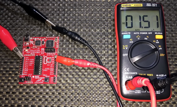
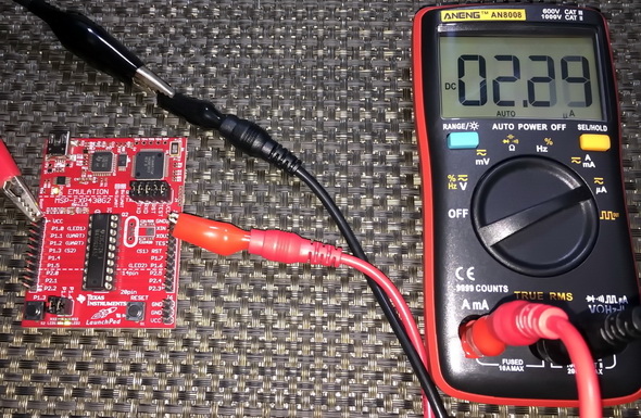
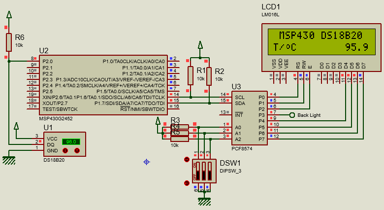
Simulation
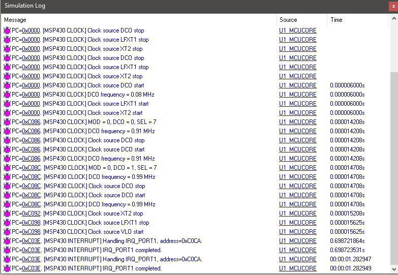
The simulation log of Proteus shown below shows when the internal oscillators started and stopped. These indicate LPM and AM states.
Explanation
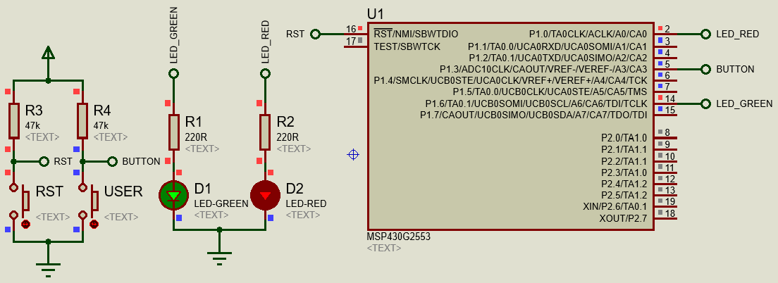
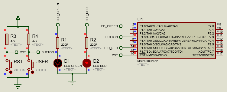
This is a pretty straight example. The code here works by first flashing the Launchpad board’s red LED for some time. During this time the MSP430 is running in active mode. After the flashing is over, the MP430 micro enters LPM2 state. Note that in LPM2 state all except the DC generator and ACLK are turned off. At this stage to wake up and exit LPM2, an interrupt is needed. Here this interrupt is generated by the external interrupt caused by pressing the Launchpad board’s user button. In the interrupt service routine (ISR), LPM2 is left and is indicated by a brief flash from the Launchpad board’s green LED. After executing the ISR, the code returns to main function and the process repeats again.
Note that for LPMs, there is no segment in Grace and LPM code definitions can be found in device’s header files.
Demo
Internal Flash Memory
In some applications, there are some very important data that we wish to retain in our target device even when it is powered down. For such purposes we need a nonvolatile memory. Like many modern micros of today’s market, MSP430s do not contain any separate EEPROM memory or battery-backed nonvolatile memory. For storing data like calibration data, settings, etc. that we would have saved in EEPROM memories, we can use the internal flash memory of our MSP430 devices. Though it may sound difficult and challenging, it is not so. However, we need to be very careful about storage locations as such that we don’t accidentally use locations where application codes reside.
Shown below is a flash memory map example of a MSP430G2xxx device.
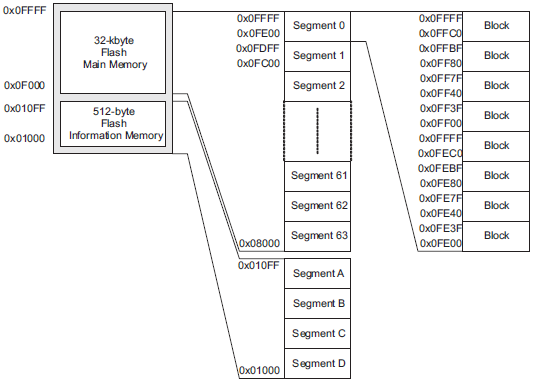
Note that there are four segments labelled A through D. These are the locations that we will be using for data storage and are called information memory. The rest is code space. We can also use the code space too but the code space has 512-byte segment size compared to 64-byte segment size of information memory. Now why is it so important to use information memory space instead of code memory? This is because of its small segment size. During memory erase, we have to erase a full segment. Bit, byte and word level read-write operations can be done easily but erasing is not possible at these levels. Two separate segments can be used to emulate low level erase. When such mechanism is applied. One segment acts like a buffer while the other is used for actual storage. Wear-leveling may optionally be applied. However, these processes add delays and extra cosing.
Segment A is a very important segment as it stores important internal calibration data like DCO frequency variables, etc. Thus, it is protected and locked separately. It will be wise to leave it and use the other three segments of information memory space to store data.
Code Example
#include <msp430.h>
#include "delay.h"
#include "SW_I2C.h"
#include "PCF8574.h"
#include "lcd.h"
void Flash_graceInit(void);
void GPIO_graceInit(void);
void BCSplus_graceInit(void);
void System_graceInit(void);
void WDTplus_graceInit(void);
void lcd_print(unsigned char x_pos, unsigned char y_pos, unsigned char value);
void Flash_Erase(unsigned int address);
void Flash_Write_Char(unsigned int address, char value);
char Flash_Read_Char(unsigned int address);
void Flash_Write_Word(unsigned int address, unsigned int value);
unsigned int Flash_Read_Word(unsigned int address);
void main(void)
{
unsigned char value = 0x00;
/* Stop watchdog timer from timing out during initial start-up. */
WDTCTL = WDTPW | WDTHOLD;
/* initialize Config for the MSP430F2xx Flash Memory Controller */
Flash_graceInit();
/* initialize Config for the MSP430 GPIO */
GPIO_graceInit();
/* initialize Config for the MSP430 2xx family clock systems (BCS) */
BCSplus_graceInit();
/* initialize Config for the MSP430 System Registers */
System_graceInit();
/* initialize Config for the MSP430 WDT+ */
WDTplus_graceInit();
LCD_init();
LCD_clear_home();
LCD_goto(0, 0);
LCD_putstr("MSP430 Flash Ex.");
value = Flash_Read_Char(0x1000);
LCD_goto(0, 1);
LCD_putstr("WR: ---");
LCD_goto(9, 1);
LCD_putstr("RD:");
lcd_print(13, 1, value);
delay_ms(2000);
while(1)
{
if((P1IN & BIT3) == !BIT3)
{
while((P1IN & BIT3) == !BIT3);
Flash_Erase(0x1000);
Flash_Write_Char(0x1000, value);
lcd_print(13, 1, value);
P1OUT |= BIT0;
_delay_cycles(40000);
P1OUT &= ~BIT0;
}
delay_ms(20);
lcd_print(4, 1, value);
value++;
delay_ms(200);
};
}
void Flash_graceInit(void)
{
/* USER CODE START (section: Flash_graceInit_prologue) */
/* User initialization code */
/* USER CODE END (section: Flash_graceInit_prologue) */
/*
* Flash Memory Control Register 2
*
* FSSEL_1 -- MCLK
* ~FN5 -- Flash controller clock divider bit 5
* FN4 -- Flash controller clock divider bit 4
* ~FN3 -- Flash controller clock divider bit 3
* FN2 -- Flash controller clock divider bit 2
* ~FN1 -- Flash controller clock divider bit 1
* FN0 -- Flash controller clock divider bit 0
*
* Note: ~<BIT> indicates that <BIT> has value zero
*/
FCTL2 = FWKEY | FSSEL_1 | FN4 | FN2 | FN0;
/* USER CODE START (section: Flash_graceInit_epilogue) */
/* User code */
/* USER CODE END (section: Flash_graceInit_epilogue) */
}
void GPIO_graceInit(void)
{
/* USER CODE START (section: GPIO_graceInit_prologue) */
/* User initialization code */
/* USER CODE END (section: GPIO_graceInit_prologue) */
/* Port 1 Output Register */
P1OUT = BIT3;
/* Port 1 Direction Register */
P1DIR = BIT0;
/* Port 1 Resistor Enable Register */
P1REN = BIT3;
/* Port 1 Interrupt Edge Select Register */
P1IES = 0;
/* Port 1 Interrupt Flag Register */
P1IFG = 0;
/* Port 2 Output Register */
P2OUT = 0;
/* Port 2 Direction Register */
P2DIR = 0;
/* Port 2 Interrupt Edge Select Register */
P2IES = 0;
/* Port 2 Interrupt Flag Register */
P2IFG = 0;
/* Port 3 Output Register */
P3OUT = 0;
/* Port 3 Direction Register */
P3DIR = 0;
/* USER CODE START (section: GPIO_graceInit_epilogue) */
/* User code */
/* USER CODE END (section: GPIO_graceInit_epilogue) */
}
void BCSplus_graceInit(void)
{
/* USER CODE START (section: BCSplus_graceInit_prologue) */
/* User initialization code */
/* USER CODE END (section: BCSplus_graceInit_prologue) */
/*
* Basic Clock System Control 2
*
* SELM_0 -- DCOCLK
* DIVM_0 -- Divide by 1
* ~SELS -- DCOCLK
* DIVS_0 -- Divide by 1
* ~DCOR -- DCO uses internal resistor
*
* Note: ~<BIT> indicates that <BIT> has value zero
*/
BCSCTL2 = SELM_0 | DIVM_0 | DIVS_0;
if (CALBC1_8MHZ != 0xFF) {
/* Adjust this accordingly to your VCC rise time */
__delay_cycles(100000);
// Follow recommended flow. First, clear all DCOx and MODx bits. Then
// apply new RSELx values. Finally, apply new DCOx and MODx bit values.
DCOCTL = 0x00;
BCSCTL1 = CALBC1_8MHZ; /* Set DCO to 8MHz */
DCOCTL = CALDCO_8MHZ;
}
/*
* Basic Clock System Control 1
*
* XT2OFF -- Disable XT2CLK
* ~XTS -- Low Frequency
* DIVA_0 -- Divide by 1
*
* Note: ~XTS indicates that XTS has value zero
*/
BCSCTL1 |= XT2OFF | DIVA_0;
/*
* Basic Clock System Control 3
*
* XT2S_0 -- 0.4 - 1 MHz
* LFXT1S_0 -- If XTS = 0, XT1 = 32768kHz Crystal ; If XTS = 1, XT1 = 0.4 - 1-MHz crystal or resonator
* XCAP_1 -- ~6 pF
*/
BCSCTL3 = XT2S_0 | LFXT1S_0 | XCAP_1;
/* USER CODE START (section: BCSplus_graceInit_epilogue) */
/* User code */
/* USER CODE END (section: BCSplus_graceInit_epilogue) */
}
void System_graceInit(void)
{
/* USER CODE START (section: System_graceInit_prologue) */
/* User initialization code */
/* USER CODE END (section: System_graceInit_prologue) */
/*
* SR, Status Register
*
* ~SCG1 -- Disable System clock generator 1
* ~SCG0 -- Disable System clock generator 0
* ~OSCOFF -- Oscillator On
* ~CPUOFF -- CPU On
* GIE -- General interrupt enable
*
* Note: ~<BIT> indicates that <BIT> has value zero
*/
__bis_SR_register(GIE);
/* USER CODE START (section: System_graceInit_epilogue) */
/* User code */
/* USER CODE END (section: System_graceInit_epilogue) */
}
void WDTplus_graceInit(void)
{
/* USER CODE START (section: RTC_B_graceInit_prologue) */
/* User initialization code */
/* USER CODE END (section: RTC_B_graceInit_prologue) */
/*
* WDTCTL, Watchdog Timer+ Register
*
* WDTPW -- Watchdog password
* WDTHOLD -- Watchdog timer+ is stopped
* ~WDTNMIES -- NMI on rising edge
* ~WDTNMI -- Reset function
* ~WDTTMSEL -- Watchdog mode
* ~WDTCNTCL -- No action
* ~WDTSSEL -- SMCLK
* ~WDTIS0 -- Watchdog clock source bit0 disabled
* ~WDTIS1 -- Watchdog clock source bit1 disabled
*
* Note: ~<BIT> indicates that <BIT> has value zero
*/
WDTCTL = WDTPW | WDTHOLD;
/* USER CODE START (section: RTC_B_graceInit_epilogue) */
/* User code */
/* USER CODE END (section: RTC_B_graceInit_epilogue) */
}
void lcd_print(unsigned char x_pos, unsigned char y_pos, unsigned char value)
{
char chr = 0x00;
chr = ((value / 100) + 0x30);
LCD_goto(x_pos, y_pos);
LCD_putchar(chr);
chr = (((value / 10) % 10) + 0x30);
LCD_goto((x_pos + 1), y_pos);
LCD_putchar(chr);
chr = ((value % 10) + 0x30);
LCD_goto((x_pos + 2), y_pos);
LCD_putchar(chr);
}
void Flash_Erase(unsigned int address)
{
char *FlashPtr;
FlashPtr = (char *)address;
FCTL1 = FWKEY + ERASE; // Set Erase bit
FCTL3 = FWKEY; // Clear Lock bit
__bic_SR_register(GIE); // Disable Interrupts
*FlashPtr = 0; // Dummy write to erase Flash segment B
while((FCTL3 & BUSY) == BUSY); // Busy
__bis_SR_register(GIE); // Enable Interrupts
FCTL1 = FWKEY; // Lock
FCTL3 = FWKEY + LOCK; // Set Lock bit
}
void Flash_Write_Char(unsigned int address, char value)
{
char *FlashPtr = (char *)address;
FCTL1 = FWKEY + WRT; // Set WRT bit for write operation
FCTL3 = FWKEY; // Clear Lock bit
__bic_SR_register(GIE); // Disable Interrupts
*FlashPtr = value; // Save Data
while((FCTL3 & BUSY) == BUSY); // Busy
__bis_SR_register(GIE); // Enable Interrupts
FCTL1 = FWKEY; // Clear WRT bit
FCTL3 = FWKEY + LOCK; // Set LOCK bit
}
char Flash_Read_Char(unsigned int address)
{
char value = 0x00;
char *FlashPtr = (char *)address;
value = *FlashPtr;
return value;
}
void Flash_Write_Word(unsigned int address, unsigned int value)
{
unsigned int *FlashPtr = (unsigned int *)address;
FCTL1 = FWKEY + WRT; // Set WRT bit for write operation
FCTL3 = FWKEY; // Clear Lock bit
__bic_SR_register(GIE); // Disable Interrupts
*FlashPtr = value; // Save Data
while((FCTL3 & BUSY) == BUSY); // Busy
__bis_SR_register(GIE); // Enable Interrupts
FCTL1 = FWKEY; // Clear WRT bit
FCTL3 = FWKEY + LOCK; // Set LOCK bit
}
unsigned int Flash_Read_Word(unsigned int address)
{
unsigned int value = 0x0000;
unsigned int *FlashPtr = (unsigned int *)address;
value = *FlashPtr;
return value;
}
Simulation

Explanation
The flash memory module of MSP430s has an integrated controller that controls programming and erase operations. The controller has four registers, a timing generator, and a voltage generator to supply program and erase voltages.
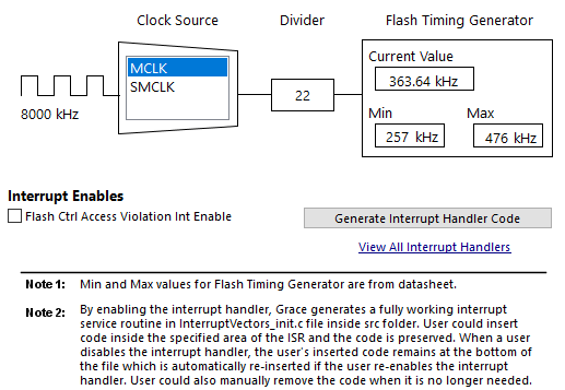
Using Grace, we initialize the aforementioned:
FCTL2 = FWKEY | FSSEL_1 | FN4 | FN2 | FN0;
To write a byte, we need two things – memory location and the value we wish to write. This memory location is that piece of memory space where we wish to store the value.
void Flash_Write_Char(unsigned int address, char value)
{
char *FlashPtr = (char *)address;
FCTL1 = FWKEY + WRT; // Set WRT bit for write operation
FCTL3 = FWKEY; // Clear Lock bit
__bic_SR_register(GIE); // Disable Interrupts
*FlashPtr = value; // Save Data
while((FCTL3 & BUSY) == BUSY); // Busy
__bis_SR_register(GIE); // Enable Interrupts
FCTL1 = FWKEY; // Clear WRT bit
FCTL3 = FWKEY + LOCK; // Set LOCK bit
}
Firstly, the address of the memory location where data is to be stored is pointed out. Flash write process starts by setting the write bit, followed by removing the flash protection. Once these are done, all interrupts are temporarily disabled to avoid any accidental write or illegal operation. The value to be written is then pointed. Until the value is successfully written all other processes are halted. Once the value to be stored is successfully written, interrupts are enabled, the write bit is cleared and the flash lock is applied.
Reading the flash is simpler. We just have to point the location we wish to read.
char Flash_Read_Char(unsigned int address)
{
char value = 0x00;
char *FlashPtr = (char *)address;
value = *FlashPtr;
return value;
}
The process for erasing is similar to write processes. The only difference is Erase bit instead of Write bit.
void Flash_Erase(unsigned int address)
{
char *FlashPtr;
FlashPtr = (char *)address;
FCTL1 = FWKEY + ERASE; // Set Erase bit
FCTL3 = FWKEY; // Clear Lock bit
__bic_SR_register(GIE); // Disable Interrupts
*FlashPtr = 0; // Dummy write to erase Flash segment B
while((FCTL3 & BUSY) == BUSY); // Busy
__bis_SR_register(GIE); // Enable Interrupts
FCTL1 = FWKEY; // Lock
FCTL3 = FWKEY + LOCK; // Set Lock bit
}
The same read-write processes can also be applied to read/write word-level values.
The code demoed her works by reading the last data stored in the target flash location (0x1000) and incrementing a variable named value. Only this location is read and updated when the Launchpad board’s button is pressed.
Demo

Time Delay Generation with Timer Compare-Match Feature
Time-bases and delays can be generated in many different ways, ranging from software techniques to using a dedicated hardware timer. Between software-based methods and hardware-based ones, the latter is more efficient and effective. This is because software-based methods rely on wasteful CPU-intensive loops and other resource-consuming processes. Hardware approaches for generating time-bases and delays are smart choices because the prime job of a timer is to count ticks or measure time. Yet within hardware-based methods, there are several techniques and tricks. We can choose between polling a free running timer or using interrupts to get things done in a more real-time sense. We have seen previously that we can use timer interrupts to time events. Here we will also see the same but this time compare-match interrupt is used instead of timer interrupt.
Code Example
#include <msp430.h>
void GPIO_graceInit(void);
void BCSplus_graceInit(void);
void Timer0_A3_graceInit(void);
void System_graceInit(void);
void WDTplus_graceInit(void);
#pragma vector = TIMER0_A0_VECTOR
__interrupt void TIMER0_A0_ISR_HOOK(void)
{
P1OUT ^= (BIT0 | BIT6);
__bic_SR_register_on_exit(LPM0_bits);
}
void main(void)
{
/* Stop watchdog timer from timing out during initial start-up. */
WDTCTL = WDTPW | WDTHOLD;
/* initialize Config for the MSP430 GPIO */
GPIO_graceInit();
/* initialize Config for the MSP430 2xx family clock systems (BCS) */
BCSplus_graceInit();
/* initialize Config for the MSP430 A3 Timer0 */
Timer0_A3_graceInit();
/* initialize Config for the MSP430 System Registers */
System_graceInit();
/* initialize Config for the MSP430 WDT+ */
WDTplus_graceInit();
P1OUT |= BIT0;
P1OUT &= ~BIT6;
while(1)
{
__bis_SR_register(LPM0_bits);
};
}
void GPIO_graceInit(void)
{
/* USER CODE START (section: GPIO_graceInit_prologue) */
/* User initialization code */
/* USER CODE END (section: GPIO_graceInit_prologue) */
/* Port 1 Output Register */
P1OUT = 0;
/* Port 1 Direction Register */
P1DIR = BIT0 | BIT6;
/* Port 1 Interrupt Edge Select Register */
P1IES = 0;
/* Port 1 Interrupt Flag Register */
P1IFG = 0;
/* Port 2 Output Register */
P2OUT = 0;
/* Port 2 Port Select Register */
P2SEL &= ~(BIT6 | BIT7);
/* Port 2 Direction Register */
P2DIR = 0;
/* Port 2 Interrupt Edge Select Register */
P2IES = 0;
/* Port 2 Interrupt Flag Register */
P2IFG = 0;
/* USER CODE START (section: GPIO_graceInit_epilogue) */
/* User code */
/* USER CODE END (section: GPIO_graceInit_epilogue) */
}
void BCSplus_graceInit(void)
{
/* USER CODE START (section: BCSplus_graceInit_prologue) */
/* User initialization code */
/* USER CODE END (section: BCSplus_graceInit_prologue) */
/*
* Basic Clock System Control 2
*
* SELM_0 -- DCOCLK
* DIVM_0 -- Divide by 1
* ~SELS -- DCOCLK
* DIVS_0 -- Divide by 1
* ~DCOR -- DCO uses internal resistor
*
* Note: ~<BIT> indicates that <BIT> has value zero
*/
BCSCTL2 = SELM_0 | DIVM_0 | DIVS_0;
if (CALBC1_1MHZ != 0xFF)
{
/* Follow recommended flow. First, clear all DCOx and MODx bits. Then
* apply new RSELx values. Finally, apply new DCOx and MODx bit values.
*/
DCOCTL = 0x00;
BCSCTL1 = CALBC1_1MHZ; /* Set DCO to 1MHz */
DCOCTL = CALDCO_1MHZ;
}
/*
* Basic Clock System Control 1
*
* XT2OFF -- Disable XT2CLK
* ~XTS -- Low Frequency
* DIVA_0 -- Divide by 1
*
* Note: ~XTS indicates that XTS has value zero
*/
BCSCTL1 |= XT2OFF | DIVA_0;
/*
* Basic Clock System Control 3
*
* XT2S_0 -- 0.4 - 1 MHz
* LFXT1S_0 -- If XTS = 0, XT1 = 32768kHz Crystal ; If XTS = 1, XT1 = 0.4 - 1-MHz crystal or resonator
* XCAP_1 -- ~6 pF
*/
BCSCTL3 = XT2S_0 | LFXT1S_0 | XCAP_1;
/* USER CODE START (section: BCSplus_graceInit_epilogue) */
/* User code */
/* USER CODE END (section: BCSplus_graceInit_epilogue) */
}
void Timer0_A3_graceInit(void)
{
/* USER CODE START (section: Timer0_A3_graceInit_prologue) */
/* User initialization code */
/* USER CODE END (section: Timer0_A3_graceInit_prologue) */
/*
* TA0CCTL0, Capture/Compare Control Register 0
*
* CM_0 -- No Capture
* CCIS_0 -- CCIxA
* ~SCS -- Asynchronous Capture
* ~SCCI -- Latched capture signal (read)
* ~CAP -- Compare mode
* OUTMOD_0 -- PWM output mode: 0 - OUT bit value
*
* Note: ~<BIT> indicates that <BIT> has value zero
*/
TA0CCTL0 = CM_0 | CCIS_0 | OUTMOD_0 | CCIE;
/* TA0CCR0, Timer_A Capture/Compare Register 0 */
TA0CCR0 = 49999;
/*
* TA0CTL, Timer_A3 Control Register
*
* TASSEL_2 -- SMCLK
* ID_3 -- Divider - /8
* MC_1 -- Up Mode
*/
TA0CTL = TASSEL_2 | ID_3 | MC_1;
/* USER CODE START (section: Timer0_A3_graceInit_epilogue) */
/* User code */
/* USER CODE END (section: Timer0_A3_graceInit_epilogue) */
}
void System_graceInit(void)
{
/* USER CODE START (section: System_graceInit_prologue) */
/* User initialization code */
/* USER CODE END (section: System_graceInit_prologue) */
/*
* SR, Status Register
*
* ~SCG1 -- Disable System clock generator 1
* ~SCG0 -- Disable System clock generator 0
* ~OSCOFF -- Oscillator On
* ~CPUOFF -- CPU On
* GIE -- General interrupt enable
*
* Note: ~<BIT> indicates that <BIT> has value zero
*/
__bis_SR_register(GIE);
/* USER CODE START (section: System_graceInit_epilogue) */
/* User code */
/* USER CODE END (section: System_graceInit_epilogue) */
}
void WDTplus_graceInit(void)
{
/* USER CODE START (section: RTC_B_graceInit_prologue) */
/* User initialization code */
/* USER CODE END (section: RTC_B_graceInit_prologue) */
/*
* WDTCTL, Watchdog Timer+ Register
*
* WDTPW -- Watchdog password
* WDTHOLD -- Watchdog timer+ is stopped
* ~WDTNMIES -- NMI on rising edge
* ~WDTNMI -- Reset function
* ~WDTTMSEL -- Watchdog mode
* ~WDTCNTCL -- No action
* ~WDTSSEL -- SMCLK
* ~WDTIS0 -- Watchdog clock source bit0 disabled
* ~WDTIS1 -- Watchdog clock source bit1 disabled
*
* Note: ~<BIT> indicates that <BIT> has value zero
*/
WDTCTL = WDTPW | WDTHOLD;
/* USER CODE START (section: RTC_B_graceInit_epilogue) */
/* User code */
/* USER CODE END (section: RTC_B_graceInit_epilogue) */
}
Simulation
Explanation
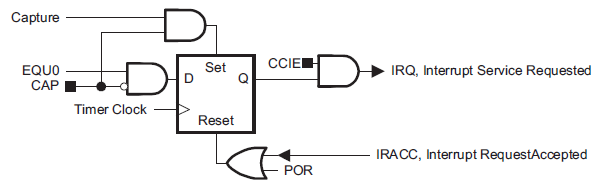
Timer0_A3 is set here for compare-match interval mode. In this mode, Timer0_A3’s settings are same as we would do for ordinary timer overflow interrupt. However, the key difference is the interrupt source. Note that in the diagram below timer overflow interrupt is not being used. Timer capture-compare interrupt is used instead.
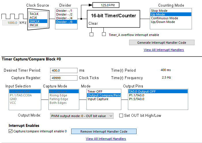
The desire time period is set for 400ms or 2.5Hz. At every 400ms interval, a compare-match interrupt will occur. How this is done? Well the timer is set for up counting and it has an input clock of 125kHz – 1MHz SMCLK prescaled by 8.
void Timer0_A3_graceInit(void)
{
/* USER CODE START (section: Timer0_A3_graceInit_prologue) */
/* User initialization code */
/* USER CODE END (section: Timer0_A3_graceInit_prologue) */
/*
* TA0CCTL0, Capture/Compare Control Register 0
*
* CM_0 -- No Capture
* CCIS_0 -- CCIxA
* ~SCS -- Asynchronous Capture
* ~SCCI -- Latched capture signal (read)
* ~CAP -- Compare mode
* OUTMOD_0 -- PWM output mode: 0 - OUT bit value
*
* Note: ~<BIT> indicates that <BIT> has value zero
*/
TA0CCTL0 = CM_0 | CCIS_0 | OUTMOD_0 | CCIE;
/* TA0CCR0, Timer_A Capture/Compare Register 0 */
TA0CCR0 = 49999;
/*
* TA0CTL, Timer_A3 Control Register
*
* TASSEL_2 -- SMCLK
* ID_3 -- Divider - /8
* MC_1 -- Up Mode
*/
TA0CTL = TASSEL_2 | ID_3 | MC_1;
/* USER CODE START (section: Timer0_A3_graceInit_epilogue) */
/* User code */
/* USER CODE END (section: Timer0_A3_graceInit_epilogue) */
}
Inside the interrupt function, the LEDs of Launchpad board are toggled. Note that after the occurrence of the interrupt LPM0 is exited.
#pragma vector = TIMER0_A0_VECTOR
__interrupt void TIMER0_A0_ISR_HOOK(void)
{
P1OUT ^= (BIT0 | BIT6);
__bic_SR_register_on_exit(LPM0_bits);
}
In the main, there is no task and in it LPM0 is entered. Thus, the process is independent of the main and is energy efficient.
while(1)
{
__bis_SR_register(LPM0_bits);
};
Demo
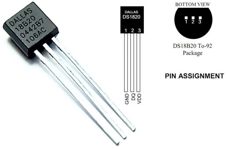
One Wire (OW) – Interfacing DS18B20 Temperature Sensor
One Wire (OW) or single wire communication is different from other more common and conventional communication platforms like SPI or I2C in terms of data exchange behavior. OW communication is also not very much popular compared to SPI, UART (RS232), I2C, RS485, etc. From device to device, the way of exchanging data varies but what’s common is the fact that all devices that use this communication method use a sort of time-slotting mechanism. Ones and zeros are defined by high pulse time over a fixed period. This trick is widely used in infrared remote controllers. One major advantage of OW communication is the fact that no special or dedicated hardware block is needed to implement it. All that is typically needed is a digital I/O pin. A timer can be used for tracking time-slots but it is optional. External interrupts can also be optionally used alongside the timer. DS18B20 one wire digital temperature sensor from Dallas semiconductor uses this communication protocol.
Code Example
one_wire.h
#include <msp430.h>
#include "delay.h"
#define DS18B20_DIR P2DIR
#define DS18B20_OUT_PORT P2OUT
#define DS18B20_IN_PORT P2IN
#define DS18B20_PIN BIT0
#define DS18B20_OUTPUT() do{DS18B20_DIR |= DS18B20_PIN;}while(0)
#define DS18B20_INPUT() do{DS18B20_DIR &= ~DS18B20_PIN;}while(0)
#define DS18B20_IN() (DS18B20_IN_PORT & DS18B20_PIN)
#define DS18B20_OUT_LOW() do{DS18B20_OUT_PORT &= ~DS18B20_PIN;}while(0)
#define DS18B20_OUT_HIGH() do{DS18B20_OUT_PORT |= DS18B20_PIN;}while(0)
#define TRUE 1
#define FALSE 0
unsigned char onewire_reset(void);
void onewire_write_bit(unsigned char bit_value);
unsigned char onewire_read_bit(void);
void onewire_write(unsigned char value);
unsigned char onewire_read(void);
one_wire.c
#include "one_wire.h"
unsigned char onewire_reset(void)
{
unsigned char res = FALSE;
DS18B20_OUTPUT();
DS18B20_OUT_LOW();
delay_us(480);
DS18B20_OUT_HIGH();
delay_us(60);
DS18B20_INPUT();
res = DS18B20_IN();
delay_us(480);
return res;
}
void onewire_write_bit(unsigned char bit_value)
{
DS18B20_OUTPUT();
DS18B20_OUT_LOW();
if(bit_value)
{
delay_us(104);
DS18B20_OUT_HIGH();
}
}
unsigned char onewire_read_bit(void)
{
DS18B20_OUTPUT();
DS18B20_OUT_LOW();
DS18B20_OUT_HIGH();
delay_us(15);
DS18B20_INPUT();
return(DS18B20_IN());
}
void onewire_write(unsigned char value)
{
unsigned char s = 0;
DS18B20_OUTPUT();
while(s < 8)
{
if((value & (1 << s)))
{
DS18B20_OUT_LOW();
_delay_cycles(1);
DS18B20_OUT_HIGH();
delay_us(60);
}
else
{
DS18B20_OUT_LOW();
delay_us(60);
DS18B20_OUT_HIGH();
_delay_cycles(1);
}
s++;
}
}
unsigned char onewire_read(void)
{
unsigned char s = 0x00;
unsigned char value = 0x00;
while(s < 8)
{
DS18B20_OUTPUT();
DS18B20_OUT_LOW();
_delay_cycles(1);
DS18B20_OUT_HIGH();
DS18B20_INPUT();
if(DS18B20_IN())
{
value |= (1 << s);
}
delay_us(60);
s++;
}
return value;
}
DS18B20.h
#include <msp430.h>
#include "delay.h"
#include "one_wire.h"
#define convert_T 0x44
#define read_scratchpad 0xBE
#define write_scratchpad 0x4E
#define copy_scratchpad 0x48
#define recall_E2 0xB8
#define read_power_supply 0xB4
#define skip_ROM 0xCC
#define resolution 12
void DS18B20_init(void);
float DS18B20_get_temperature(void);
DS18B20.c
#include "DS18B20.h"
void DS18B20_init(void)
{
onewire_reset();
delay_ms(100);
}
float DS18B20_get_temperature(void)
{
unsigned char msb = 0x00;
unsigned char lsb = 0x00;
register float temp = 0.0;
onewire_reset();
onewire_write(skip_ROM);
onewire_write(convert_T);
switch(resolution)
{
case 12:
{
delay_ms(750);
break;
}
case 11:
{
delay_ms(375);
break;
}
case 10:
{
delay_ms(188);
break;
}
case 9:
{
delay_ms(94);
break;
}
}
onewire_reset();
onewire_write(skip_ROM);
onewire_write(read_scratchpad);
lsb = onewire_read();
msb = onewire_read();
temp = msb;
temp *= 256.0;
temp += lsb;
switch(resolution)
{
case 12:
{
temp *= 0.0625;
break;
}
case 11:
{
temp *= 0.125;
break;
}
case 10:
{
temp *= 0.25;
break;
}
case 9:
{
temp *= 0.5;
break;
}
}
delay_ms(40);
return (temp);
}
main.c
#include <msp430.h>
#include "delay.h"
#include "SW_I2C.h"
#include "PCF8574.h"
#include "one_wire.h"
#include "DS18B20.h"
#include "lcd.h"
const unsigned char symbol[8] =
{
0x00, 0x06, 0x09, 0x09, 0x06, 0x00, 0x00, 0x00
};
void GPIO_graceInit(void);
void BCSplus_graceInit(void);
void System_graceInit(void);
void WDTplus_graceInit(void);
void lcd_symbol(void);
void print_C(unsigned char x_pos, unsigned char y_pos, signed int value);
void print_I(unsigned char x_pos, unsigned char y_pos, signed long value);
void print_D(unsigned char x_pos, unsigned char y_pos, signed int value, unsigned char points);
void print_F(unsigned char x_pos, unsigned char y_pos, float value, unsigned char points);
void main(void)
{
float t = 0.0;
/* Stop watchdog timer from timing out during initial start-up. */
WDTCTL = WDTPW | WDTHOLD;
/* initialize Config for the MSP430 GPIO */
GPIO_graceInit();
/* initialize Config for the MSP430 2xx family clock systems (BCS) */
BCSplus_graceInit();
/* initialize Config for the MSP430 System Registers */
System_graceInit();
/* initialize Config for the MSP430 WDT+ */
WDTplus_graceInit();
DS18B20_init();
LCD_init();
lcd_symbol();
LCD_goto(1, 0);
LCD_putstr("MSP430 DS18B20");
LCD_goto(0, 1);
LCD_putstr("T/ C");
LCD_goto(2, 1);
LCD_send(0, DAT);
while(1)
{
t = DS18B20_get_temperature();
print_F(9, 1, t, 3);
delay_ms(1000);
};
}
void GPIO_graceInit(void)
{
/* USER CODE START (section: GPIO_graceInit_prologue) */
/* User initialization code */
/* USER CODE END (section: GPIO_graceInit_prologue) */
/* Port 1 Output Register */
P1OUT = 0;
/* Port 1 Direction Register */
P1DIR = 0;
/* Port 1 Interrupt Edge Select Register */
P1IES = 0;
/* Port 1 Interrupt Flag Register */
P1IFG = 0;
/* Port 2 Output Register */
P2OUT = 0;
/* Port 2 Port Select Register */
P2SEL &= ~(BIT6 | BIT7);
/* Port 2 Direction Register */
P2DIR = 0;
/* Port 2 Interrupt Edge Select Register */
P2IES = 0;
/* Port 2 Interrupt Flag Register */
P2IFG = 0;
/* USER CODE START (section: GPIO_graceInit_epilogue) */
/* User code */
/* USER CODE END (section: GPIO_graceInit_epilogue) */
}
void BCSplus_graceInit(void)
{
/* USER CODE START (section: BCSplus_graceInit_prologue) */
/* User initialization code */
/* USER CODE END (section: BCSplus_graceInit_prologue) */
/*
* Basic Clock System Control 2
*
* SELM_0 -- DCOCLK
* DIVM_0 -- Divide by 1
* ~SELS -- DCOCLK
* DIVS_0 -- Divide by 1
* ~DCOR -- DCO uses internal resistor
*
* Note: ~<BIT> indicates that <BIT> has value zero
*/
BCSCTL2 = SELM_0 | DIVM_0 | DIVS_0;
if (CALBC1_8MHZ != 0xFF)
{
/* Adjust this accordingly to your VCC rise time */
__delay_cycles(100000);
// Follow recommended flow. First, clear all DCOx and MODx bits. Then
// apply new RSELx values. Finally, apply new DCOx and MODx bit values.
DCOCTL = 0x00;
BCSCTL1 = CALBC1_8MHZ; /* Set DCO to 8MHz */
DCOCTL = CALDCO_8MHZ;
}
/*
* Basic Clock System Control 1
*
* XT2OFF -- Disable XT2CLK
* ~XTS -- Low Frequency
* DIVA_0 -- Divide by 1
*
* Note: ~XTS indicates that XTS has value zero
*/
BCSCTL1 |= XT2OFF | DIVA_0;
/*
* Basic Clock System Control 3
*
* XT2S_0 -- 0.4 - 1 MHz
* LFXT1S_0 -- If XTS = 0, XT1 = 32768kHz Crystal ; If XTS = 1, XT1 = 0.4 - 1-MHz crystal or resonator
* XCAP_1 -- ~6 pF
*/
BCSCTL3 = XT2S_0 | LFXT1S_0 | XCAP_1;
/* USER CODE START (section: BCSplus_graceInit_epilogue) */
/* User code */
/* USER CODE END (section: BCSplus_graceInit_epilogue) */
}
void System_graceInit(void)
{
/* USER CODE START (section: System_graceInit_prologue) */
/* User initialization code */
/* USER CODE END (section: System_graceInit_prologue) */
/*
* SR, Status Register
*
* ~SCG1 -- Disable System clock generator 1
* ~SCG0 -- Disable System clock generator 0
* ~OSCOFF -- Oscillator On
* ~CPUOFF -- CPU On
* GIE -- General interrupt enable
*
* Note: ~<BIT> indicates that <BIT> has value zero
*/
__bis_SR_register(GIE);
/* USER CODE START (section: System_graceInit_epilogue) */
/* User code */
/* USER CODE END (section: System_graceInit_epilogue) */
}
void WDTplus_graceInit(void)
{
/* USER CODE START (section: RTC_B_graceInit_prologue) */
/* User initialization code */
/* USER CODE END (section: RTC_B_graceInit_prologue) */
/*
* WDTCTL, Watchdog Timer+ Register
*
* WDTPW -- Watchdog password
* WDTHOLD -- Watchdog timer+ is stopped
* ~WDTNMIES -- NMI on rising edge
* ~WDTNMI -- Reset function
* ~WDTTMSEL -- Watchdog mode
* ~WDTCNTCL -- No action
* ~WDTSSEL -- SMCLK
* ~WDTIS0 -- Watchdog clock source bit0 disabled
* ~WDTIS1 -- Watchdog clock source bit1 disabled
*
* Note: ~<BIT> indicates that <BIT> has value zero
*/
WDTCTL = WDTPW | WDTHOLD;
/* USER CODE START (section: RTC_B_graceInit_epilogue) */
/* User code */
/* USER CODE END (section: RTC_B_graceInit_epilogue) */
}
void lcd_symbol(void)
{
unsigned char s = 0;
LCD_send(0x40, CMD);
for(s = 0; s < 8; s++)
{
LCD_send(symbol[s], DAT);
}
LCD_send(0x80, CMD);
}
void print_C(unsigned char x_pos, unsigned char y_pos, signed int value)
{
char ch[5] = {0x20, 0x20, 0x20, 0x20, '\0'};
if(value < 0x00)
{
ch[0] = 0x2D;
value = -value;
}
else
{
ch[0] = 0x20;
}
if((value > 99) && (value <= 999))
{
ch[1] = ((value / 100) + 0x30);
ch[2] = (((value % 100) / 10) + 0x30);
ch[3] = ((value % 10) + 0x30);
}
else if((value > 9) && (value <= 99))
{
ch[1] = (((value % 100) / 10) + 0x30);
ch[2] = ((value % 10) + 0x30);
ch[3] = 0x20;
}
else if((value >= 0) && (value <= 9))
{
ch[1] = ((value % 10) + 0x30);
ch[2] = 0x20;
ch[3] = 0x20;
}
LCD_goto(x_pos, y_pos);
LCD_putstr(ch);
}
void print_I(unsigned char x_pos, unsigned char y_pos, signed long value)
{
char ch[7] = {0x20, 0x20, 0x20, 0x20, 0x20, 0x20, '\0'};
if(value < 0)
{
ch[0] = 0x2D;
value = -value;
}
else
{
ch[0] = 0x20;
}
if(value > 9999)
{
ch[1] = ((value / 10000) + 0x30);
ch[2] = (((value % 10000)/ 1000) + 0x30);
ch[3] = (((value % 1000) / 100) + 0x30);
ch[4] = (((value % 100) / 10) + 0x30);
ch[5] = ((value % 10) + 0x30);
}
else if((value > 999) && (value <= 9999))
{
ch[1] = (((value % 10000)/ 1000) + 0x30);
ch[2] = (((value % 1000) / 100) + 0x30);
ch[3] = (((value % 100) / 10) + 0x30);
ch[4] = ((value % 10) + 0x30);
ch[5] = 0x20;
}
else if((value > 99) && (value <= 999))
{
ch[1] = (((value % 1000) / 100) + 0x30);
ch[2] = (((value % 100) / 10) + 0x30);
ch[3] = ((value % 10) + 0x30);
ch[4] = 0x20;
ch[5] = 0x20;
}
else if((value > 9) && (value <= 99))
{
ch[1] = (((value % 100) / 10) + 0x30);
ch[2] = ((value % 10) + 0x30);
ch[3] = 0x20;
ch[4] = 0x20;
ch[5] = 0x20;
}
else
{
ch[1] = ((value % 10) + 0x30);
ch[2] = 0x20;
ch[3] = 0x20;
ch[4] = 0x20;
ch[5] = 0x20;
}
LCD_goto(x_pos, y_pos);
LCD_putstr(ch);
}
void print_D(unsigned char x_pos, unsigned char y_pos, signed int value, unsigned char points)
{
char ch[5] = {0x2E, 0x20, 0x20, '\0'};
ch[1] = ((value / 100) + 0x30);
if(points > 1)
{
ch[2] = (((value / 10) % 10) + 0x30);
if(points > 1)
{
ch[3] = ((value % 10) + 0x30);
}
}
LCD_goto(x_pos, y_pos);
LCD_putstr(ch);
}
void print_F(unsigned char x_pos, unsigned char y_pos, float value, unsigned char points)
{
signed long tmp = 0x0000;
tmp = value;
print_I(x_pos, y_pos, tmp);
tmp = ((value - tmp) * 1000);
if(tmp < 0)
{
tmp = -tmp;
}
if(value < 0)
{
value = -value;
LCD_goto(x_pos, y_pos);
LCD_putchar(0x2D);
}
else
{
LCD_goto(x_pos, y_pos);
LCD_putchar(0x20);
}
if((value >= 10000) && (value < 100000))
{
print_D((x_pos + 6), y_pos, tmp, points);
}
else if((value >= 1000) && (value < 10000))
{
print_D((x_pos + 5), y_pos, tmp, points);
}
else if((value >= 100) && (value < 1000))
{
print_D((x_pos + 4), y_pos, tmp, points);
}
else if((value >= 10) && (value < 100))
{
print_D((x_pos + 3), y_pos, tmp, points);
}
else if(value < 10)
{
print_D((x_pos + 2), y_pos, tmp, points);
}
}
Simulation
Explanation
One wire communication is detailed in these application notes from Maxim:
https://www.maximintegrated.com/en/app-notes/index.mvp/id/126
https://www.maximintegrated.com/en/app-notes/index.mvp/id/162
These notes are all that are needed for implementing the one wire communication interface for DS18B20. Please go through these notes for details. The codes are self-explanatory and are implemented from the code examples in these app notes.
Demo

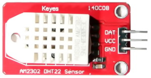
One Wire (OW) – Interfacing DHT22 Hygrometer Sensor
Like DS18B20, DHT22 (a.k.a AM2302) digital relative humidity-temperature or hygrometer sensor uses time-slotting principle over one wire to transfer data to its host controller. Apart from other technical specs, these sensors differ in terms of time-slots and in the process of data exchanging and communication bus arbitration. Since data is transferred digitally over one wire, there is no need for such sensors to be present on board and close to the host MCU. Thus, such sensors can be placed significantly far from the host micro. This is not so easily possible with analog sensors or with sensors using multiple wires. This feature is what makes OW communication method an impressive one.
Code Example
DHT22.h
#include <msp430.h>
#include <delay.h>
#define DHT22_DIR P2DIR
#define DHT22_OUT_PORT P2OUT
#define DHT22_IN_PORT P2IN
#define DHT22_PIN BIT0
#define DHT22_DIR_OUT() do{DHT22_DIR |= DHT22_PIN;}while(0)
#define DHT22_DIR_IN() do{DHT22_DIR &= ~DHT22_PIN;}while(0)
#define DHT22_IN() (DHT22_IN_PORT & DHT22_PIN)
#define DHT22_OUT_LOW() do{DHT22_OUT_PORT &= ~DHT22_PIN;}while(0)
#define DHT22_OUT_HIGH() do{DHT22_OUT_PORT |= DHT22_PIN;}while(0)
#define TRUE 1
#define FALSE 0
extern unsigned char values[5];
void DHT22_init(void);
unsigned char DHT22_get_byte(void);
unsigned char DHT22_get_data(void);
DHT22.c
#include "DHT22.h"
unsigned char values[5];
void DHT22_init(void)
{
DHT22_DIR_IN();
delay_ms(1000);
}
unsigned char DHT22_get_byte(void)
{
unsigned char s = 8;
unsigned char value = 0;
DHT22_DIR_IN();
while(s > 0)
{
value <<= 1;
while(DHT22_IN() == FALSE);
delay_us(30);
if(DHT22_IN())
{
value |= 1;
}
while(DHT22_IN());
s--;
}
return value;
}
unsigned char DHT22_get_data(void)
{
unsigned char chk = FALSE;
unsigned char s = 0;
unsigned char check_sum = 0;
DHT22_DIR_OUT();
DHT22_OUT_HIGH();
DHT22_OUT_LOW();
delay_ms(1);
DHT22_OUT_HIGH();
delay_us(32);
DHT22_DIR_IN();
chk = DHT22_IN();
delay_us(2);
if(chk == TRUE)
{
return 1;
}
delay_us(80);
chk = DHT22_IN();
if(chk == FALSE)
{
return 2;
}
delay_us(80);
for(s = 0; s <= 4; s += 1)
{
values[s] = DHT22_get_byte();
}
DHT22_DIR_OUT();
DHT22_OUT_HIGH();
for(s = 0; s < 4; s++)
{
check_sum += values[s];
}
if(check_sum != values[4])
{
return 3;
}
else
{
return 0;
}
}
main.c
#include <msp430.h>
#include "delay.h"
#include "SW_I2C.h"
#include "PCF8574.h"
#include "lcd.h"
#include "DHT22.h"
const unsigned char symbol[8] =
{
0x00, 0x06, 0x09, 0x09, 0x06, 0x00, 0x00, 0x00
};
void GPIO_graceInit(void);
void BCSplus_graceInit(void);
void System_graceInit(void);
void WDTplus_graceInit(void);
void lcd_symbol(void);
void print_C(unsigned char x_pos, unsigned char y_pos, signed int value);
void print_I(unsigned char x_pos, unsigned char y_pos, signed long value);
void print_D(unsigned char x_pos, unsigned char y_pos, signed int value, unsigned char points);
void print_F(unsigned char x_pos, unsigned char y_pos, float value, unsigned char points);
void main(void)
{
float value = 0.0;
unsigned char state = 0;
/* Stop watchdog timer from timing out during initial start-up. */
WDTCTL = WDTPW | WDTHOLD;
/* initialize Config for the MSP430 GPIO */
GPIO_graceInit();
/* initialize Config for the MSP430 2xx family clock systems (BCS) */
BCSplus_graceInit();
/* initialize Config for the MSP430 System Registers */
System_graceInit();
/* initialize Config for the MSP430 WDT+ */
WDTplus_graceInit();
DHT22_init();
LCD_init();
lcd_symbol();
while(1)
{
state = DHT22_get_data();
switch(state)
{
case 1:
{
LCD_goto(0, 0);
LCD_putstr("No Sensor Found!");
LCD_goto(0, 1);
LCD_putstr(" ");
break;
}
case 2:
{
LCD_goto(0, 0);
LCD_putstr("Checksum Error!");
LCD_goto(0, 1);
LCD_putstr(" ");
break;
}
default:
{
value = ((values[0] * 256.0 + values[1]) * 0.1);
LCD_goto(0, 0);
LCD_putstr("R.H/%: ");
print_F(11, 0, value, 1);
value = ((values[2] * 256.0 + values[3]) * 0.1);
LCD_goto(0, 1);
LCD_putstr("T/ C : ");
LCD_goto(2, 1);
LCD_send(0, DAT);
print_F(11, 1, value, 1);
break;
}
}
delay_ms(1000);
};
}
void GPIO_graceInit(void)
{
/* USER CODE START (section: GPIO_graceInit_prologue) */
/* User initialization code */
/* USER CODE END (section: GPIO_graceInit_prologue) */
/* Port 1 Output Register */
P1OUT = 0;
/* Port 1 Direction Register */
P1DIR = 0;
/* Port 1 Interrupt Edge Select Register */
P1IES = 0;
/* Port 1 Interrupt Flag Register */
P1IFG = 0;
/* Port 2 Output Register */
P2OUT = 0;
/* Port 2 Port Select Register */
P2SEL &= ~(BIT6 | BIT7);
/* Port 2 Direction Register */
P2DIR = 0;
/* Port 2 Interrupt Edge Select Register */
P2IES = 0;
/* Port 2 Interrupt Flag Register */
P2IFG = 0;
/* USER CODE START (section: GPIO_graceInit_epilogue) */
/* User code */
/* USER CODE END (section: GPIO_graceInit_epilogue) */
}
void BCSplus_graceInit(void)
{
/* USER CODE START (section: BCSplus_graceInit_prologue) */
/* User initialization code */
/* USER CODE END (section: BCSplus_graceInit_prologue) */
/*
* Basic Clock System Control 2
*
* SELM_0 -- DCOCLK
* DIVM_0 -- Divide by 1
* ~SELS -- DCOCLK
* DIVS_0 -- Divide by 1
* ~DCOR -- DCO uses internal resistor
*
* Note: ~<BIT> indicates that <BIT> has value zero
*/
BCSCTL2 = SELM_0 | DIVM_0 | DIVS_0;
if (CALBC1_8MHZ != 0xFF)
{
/* Adjust this accordingly to your VCC rise time */
__delay_cycles(100000);
// Follow recommended flow. First, clear all DCOx and MODx bits. Then
// apply new RSELx values. Finally, apply new DCOx and MODx bit values.
DCOCTL = 0x00;
BCSCTL1 = CALBC1_8MHZ; /* Set DCO to 8MHz */
DCOCTL = CALDCO_8MHZ;
}
/*
* Basic Clock System Control 1
*
* XT2OFF -- Disable XT2CLK
* ~XTS -- Low Frequency
* DIVA_0 -- Divide by 1
*
* Note: ~XTS indicates that XTS has value zero
*/
BCSCTL1 |= XT2OFF | DIVA_0;
/*
* Basic Clock System Control 3
*
* XT2S_0 -- 0.4 - 1 MHz
* LFXT1S_0 -- If XTS = 0, XT1 = 32768kHz Crystal ; If XTS = 1, XT1 = 0.4 - 1-MHz crystal or resonator
* XCAP_1 -- ~6 pF
*/
BCSCTL3 = XT2S_0 | LFXT1S_0 | XCAP_1;
/* USER CODE START (section: BCSplus_graceInit_epilogue) */
/* User code */
/* USER CODE END (section: BCSplus_graceInit_epilogue) */
}
void System_graceInit(void)
{
/* USER CODE START (section: System_graceInit_prologue) */
/* User initialization code */
/* USER CODE END (section: System_graceInit_prologue) */
/*
* SR, Status Register
*
* ~SCG1 -- Disable System clock generator 1
* ~SCG0 -- Disable System clock generator 0
* ~OSCOFF -- Oscillator On
* ~CPUOFF -- CPU On
* GIE -- General interrupt enable
*
* Note: ~<BIT> indicates that <BIT> has value zero
*/
__bis_SR_register(GIE);
/* USER CODE START (section: System_graceInit_epilogue) */
/* User code */
/* USER CODE END (section: System_graceInit_epilogue) */
}
void WDTplus_graceInit(void)
{
/* USER CODE START (section: RTC_B_graceInit_prologue) */
/* User initialization code */
/* USER CODE END (section: RTC_B_graceInit_prologue) */
/*
* WDTCTL, Watchdog Timer+ Register
*
* WDTPW -- Watchdog password
* WDTHOLD -- Watchdog timer+ is stopped
* ~WDTNMIES -- NMI on rising edge
* ~WDTNMI -- Reset function
* ~WDTTMSEL -- Watchdog mode
* ~WDTCNTCL -- No action
* ~WDTSSEL -- SMCLK
* ~WDTIS0 -- Watchdog clock source bit0 disabled
* ~WDTIS1 -- Watchdog clock source bit1 disabled
*
* Note: ~<BIT> indicates that <BIT> has value zero
*/
WDTCTL = WDTPW | WDTHOLD;
/* USER CODE START (section: RTC_B_graceInit_epilogue) */
/* User code */
/* USER CODE END (section: RTC_B_graceInit_epilogue) */
}
void lcd_symbol(void)
{
unsigned char s = 0;
LCD_send(0x40, CMD);
for(s = 0; s < 8; s++)
{
LCD_send(symbol[s], DAT);
}
LCD_send(0x80, CMD);
}
void print_C(unsigned char x_pos, unsigned char y_pos, signed int value)
{
char ch[5] = {0x20, 0x20, 0x20, 0x20, '\0'};
if(value < 0x00)
{
ch[0] = 0x2D;
value = -value;
}
else
{
ch[0] = 0x20;
}
if((value > 99) && (value <= 999))
{
ch[1] = ((value / 100) + 0x30);
ch[2] = (((value % 100) / 10) + 0x30);
ch[3] = ((value % 10) + 0x30);
}
else if((value > 9) && (value <= 99))
{
ch[1] = (((value % 100) / 10) + 0x30);
ch[2] = ((value % 10) + 0x30);
ch[3] = 0x20;
}
else if((value >= 0) && (value <= 9))
{
ch[1] = ((value % 10) + 0x30);
ch[2] = 0x20;
ch[3] = 0x20;
}
LCD_goto(x_pos, y_pos);
LCD_putstr(ch);
}
void print_I(unsigned char x_pos, unsigned char y_pos, signed long value)
{
char ch[7] = {0x20, 0x20, 0x20, 0x20, 0x20, 0x20, '\0'};
if(value < 0)
{
ch[0] = 0x2D;
value = -value;
}
else
{
ch[0] = 0x20;
}
if(value > 9999)
{
ch[1] = ((value / 10000) + 0x30);
ch[2] = (((value % 10000)/ 1000) + 0x30);
ch[3] = (((value % 1000) / 100) + 0x30);
ch[4] = (((value % 100) / 10) + 0x30);
ch[5] = ((value % 10) + 0x30);
}
else if((value > 999) && (value <= 9999))
{
ch[1] = (((value % 10000)/ 1000) + 0x30);
ch[2] = (((value % 1000) / 100) + 0x30);
ch[3] = (((value % 100) / 10) + 0x30);
ch[4] = ((value % 10) + 0x30);
ch[5] = 0x20;
}
else if((value > 99) && (value <= 999))
{
ch[1] = (((value % 1000) / 100) + 0x30);
ch[2] = (((value % 100) / 10) + 0x30);
ch[3] = ((value % 10) + 0x30);
ch[4] = 0x20;
ch[5] = 0x20;
}
else if((value > 9) && (value <= 99))
{
ch[1] = (((value % 100) / 10) + 0x30);
ch[2] = ((value % 10) + 0x30);
ch[3] = 0x20;
ch[4] = 0x20;
ch[5] = 0x20;
}
else
{
ch[1] = ((value % 10) + 0x30);
ch[2] = 0x20;
ch[3] = 0x20;
ch[4] = 0x20;
ch[5] = 0x20;
}
LCD_goto(x_pos, y_pos);
LCD_putstr(ch);
}
void print_D(unsigned char x_pos, unsigned char y_pos, signed int value, unsigned char points)
{
char ch[5] = {0x2E, 0x20, 0x20, '\0'};
ch[1] = ((value / 100) + 0x30);
if(points > 1)
{
ch[2] = (((value / 10) % 10) + 0x30);
if(points > 1)
{
ch[3] = ((value % 10) + 0x30);
}
}
LCD_goto(x_pos, y_pos);
LCD_putstr(ch);
}
void print_F(unsigned char x_pos, unsigned char y_pos, float value, unsigned char points)
{
signed long tmp = 0x0000;
tmp = value;
print_I(x_pos, y_pos, tmp);
tmp = ((value - tmp) * 1000);
if(tmp < 0)
{
tmp = -tmp;
}
if(value < 0)
{
value = -value;
LCD_goto(x_pos, y_pos);
LCD_putchar(0x2D);
}
else
{
LCD_goto(x_pos, y_pos);
LCD_putchar(0x20);
}
if((value >= 10000) && (value < 100000))
{
print_D((x_pos + 6), y_pos, tmp, points);
}
else if((value >= 1000) && (value < 10000))
{
print_D((x_pos + 5), y_pos, tmp, points);
}
else if((value >= 100) && (value < 1000))
{
print_D((x_pos + 4), y_pos, tmp, points);
}
else if((value >= 10) && (value < 100))
{
print_D((x_pos + 3), y_pos, tmp, points);
}
else if(value < 10)
{
print_D((x_pos + 2), y_pos, tmp, points);
}
}
Explanation
Unlike I2C, SPI, UART and other communication methods, one wire communication has no fixed communication standard. A perfect example is the difference between the way of communicating with DHT22 and DS18B20. Although they appear to share a similar methodology but the communication protocols are different.
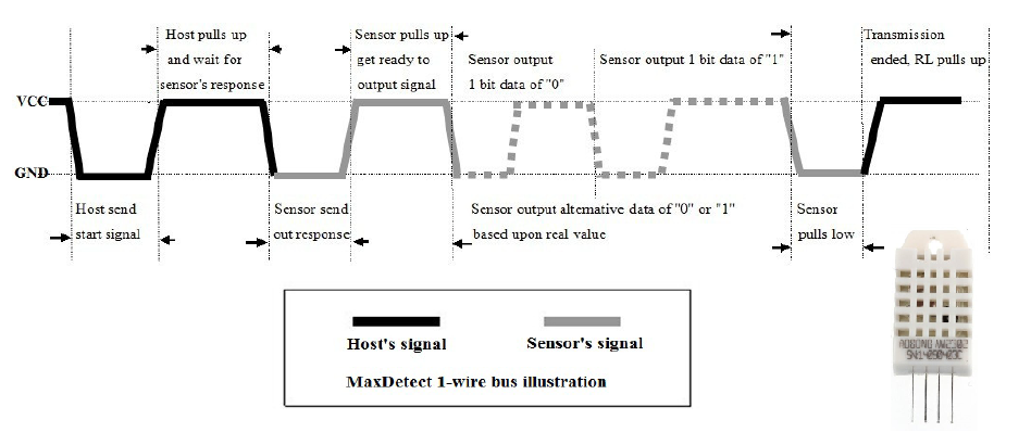
Shown above is the timing diagram of DHT22. If you compare the timings for ones and zeroes in both devices you’ll notice that these timings are way different. Same goes for the data, command and control processes. Here again the datasheet of DHT22 is used to create the library for DHT22 and the process is just manipulation of a single GPIO pin.
Demo

Software UART
Software UART is seldom needed but it comes really useful in absence of hardware UART. In some cases, we may not have the luxury of using hardware UART. Hardware UART block may also be absent. We already know that USCI module can be used for implementing hardware UART but this block is not present in chips like MSP430G2452. In such devices, we have to use software-generated UART. Software UART uses ordinary digital I/Os and delays. Both additionally and optionally external interrupts and timers can be used for better results. Owing to its hardware independency and simplicity, it is very robust. However extra coding and therefore extra memory spaces are needed.
Code Example
SW_UART.h
#include <msp430.h>
#include "delay.h"
#define SW_UART_RXD_DIR P1DIR
#define SW_UART_TXD_DIR P1DIR
#define SW_UART_RXD_OUT P1OUT
#define SW_UART_TXD_OUT P1OUT
#define SW_UART_RXD_IN P1IN
#define SW_UART_RXD_IN_RES P1REN
#define SW_UART_RXD_PIN BIT1
#define SW_UART_TXD_PIN BIT2
#define SW_UART_RXD_DIR_IN() do{SW_UART_RXD_OUT |= SW_UART_RXD_PIN; SW_UART_RXD_DIR &= ~SW_UART_RXD_PIN; SW_UART_RXD_IN_RES |= SW_UART_RXD_PIN;}while(0)
#define SW_UART_TXD_DIR_OUT() do{SW_UART_TXD_DIR |= SW_UART_TXD_PIN;}while(0)
#define SW_UART_TXD_OUT_HIGH() do{SW_UART_TXD_OUT |= SW_UART_TXD_PIN;}while(0)
#define SW_UART_TXD_OUT_LOW() do{SW_UART_TXD_OUT &= ~SW_UART_TXD_PIN;}while(0)
#define SW_UART_RXD_INPUT() (SW_UART_RXD_IN & SW_UART_RXD_PIN)
#define baudrate 4800
#define no_of_bits 8
#define one_bit_delay (1000000 / baudrate)
#define half_bit_delay (one_bit_delay / 2)
void SW_UART_init(void);
void SW_UART_transmit(unsigned char value);
unsigned char SW_UART_receive(void);
SW_UART.c
#include "SW_UART.h"
void SW_UART_init(void)
{
SW_UART_TXD_DIR_OUT();
SW_UART_RXD_DIR_IN();
SW_UART_TXD_OUT_HIGH();
delay_ms(10);
}
void SW_UART_transmit(unsigned char value)
{
unsigned char bits = 0;
SW_UART_TXD_OUT_LOW();
delay_us(one_bit_delay);
for(bits = 0; bits < no_of_bits; bits++)
{
if((value >> bits) & 0x01)
{
SW_UART_TXD_OUT_HIGH();
}
else
{
SW_UART_TXD_OUT_LOW();
}
delay_us(one_bit_delay);
};
SW_UART_TXD_OUT_HIGH();
delay_us(one_bit_delay);
}
unsigned char SW_UART_receive(void)
{
unsigned char bits = 0;
unsigned char value = 0;
while(SW_UART_RXD_INPUT());
delay_us(one_bit_delay);
delay_us(half_bit_delay);
for(bits = 0; bits < no_of_bits; bits++)
{
if(SW_UART_RXD_INPUT())
{
value += (1 << bits);
}
delay_us(one_bit_delay);
};
if(SW_UART_RXD_INPUT())
{
delay_us(half_bit_delay);
return value;
}
else
{
delay_us(half_bit_delay);
return 0;
}
}
main.c
#include <msp430.h>
#include "delay.h"
#include "SW_I2C.h"
#include "PCF8574.h"
#include "lcd.h"
#include "SW_UART.h"
void GPIO_graceInit(void);
void BCSplus_graceInit(void);
void System_graceInit(void);
void WDTplus_graceInit(void);
void main(void)
{
unsigned char rx_value = 0x00;
unsigned char tx_value = 0x20;
/* Stop watchdog timer from timing out during initial start-up. */
WDTCTL = WDTPW | WDTHOLD;
/* initialize Config for the MSP430 GPIO */
GPIO_graceInit();
/* initialize Config for the MSP430 2xx family clock systems (BCS) */
BCSplus_graceInit();
/* initialize Config for the MSP430 System Registers */
System_graceInit();
/* initialize Config for the MSP430 WDT+ */
WDTplus_graceInit();
LCD_init();
LCD_clear_home();
LCD_goto(0, 0);
LCD_putstr("TXD:");
LCD_goto(0, 1);
LCD_putstr("RXD:");
SW_UART_init();
while(1)
{
rx_value = SW_UART_receive();
LCD_goto(15, 0);
LCD_putchar(rx_value);
tx_value++;
LCD_goto(15, 1);
LCD_putchar(tx_value);
SW_UART_transmit(tx_value);
delay_ms(200);
};
}
void GPIO_graceInit(void)
{
/* USER CODE START (section: GPIO_graceInit_prologue) */
/* User initialization code */
/* USER CODE END (section: GPIO_graceInit_prologue) */
/* Port 1 Output Register */
P1OUT = 0;
/* Port 1 Direction Register */
P1DIR = 0;
/* Port 1 Interrupt Edge Select Register */
P1IES = 0;
/* Port 1 Interrupt Flag Register */
P1IFG = 0;
/* Port 2 Output Register */
P2OUT = 0;
/* Port 2 Direction Register */
P2DIR = 0;
/* Port 2 Interrupt Edge Select Register */
P2IES = 0;
/* Port 2 Interrupt Flag Register */
P2IFG = 0;
/* USER CODE START (section: GPIO_graceInit_epilogue) */
/* User code */
/* USER CODE END (section: GPIO_graceInit_epilogue) */
}
void BCSplus_graceInit(void)
{
/* USER CODE START (section: BCSplus_graceInit_prologue) */
/* User initialization code */
/* USER CODE END (section: BCSplus_graceInit_prologue) */
/*
* Basic Clock System Control 2
*
* SELM_0 -- DCOCLK
* DIVM_0 -- Divide by 1
* ~SELS -- DCOCLK
* DIVS_0 -- Divide by 1
* ~DCOR -- DCO uses internal resistor
*
* Note: ~<BIT> indicates that <BIT> has value zero
*/
BCSCTL2 = SELM_0 | DIVM_0 | DIVS_0;
if (CALBC1_8MHZ != 0xFF) {
/* Adjust this accordingly to your VCC rise time */
__delay_cycles(100000);
// Follow recommended flow. First, clear all DCOx and MODx bits. Then
// apply new RSELx values. Finally, apply new DCOx and MODx bit values.
DCOCTL = 0x00;
BCSCTL1 = CALBC1_8MHZ; /* Set DCO to 8MHz */
DCOCTL = CALDCO_8MHZ;
}
/*
* Basic Clock System Control 1
*
* XT2OFF -- Disable XT2CLK
* ~XTS -- Low Frequency
* DIVA_0 -- Divide by 1
*
* Note: ~XTS indicates that XTS has value zero
*/
BCSCTL1 |= XT2OFF | DIVA_0;
/*
* Basic Clock System Control 3
*
* XT2S_0 -- 0.4 - 1 MHz
* LFXT1S_0 -- If XTS = 0, XT1 = 32768kHz Crystal ; If XTS = 1, XT1 = 0.4 - 1-MHz crystal or resonator
* XCAP_1 -- ~6 pF
*/
BCSCTL3 = XT2S_0 | LFXT1S_0 | XCAP_1;
/* USER CODE START (section: BCSplus_graceInit_epilogue) */
/* User code */
/* USER CODE END (section: BCSplus_graceInit_epilogue) */
}
void System_graceInit(void)
{
/* USER CODE START (section: System_graceInit_prologue) */
/* User initialization code */
/* USER CODE END (section: System_graceInit_prologue) */
/*
* SR, Status Register
*
* ~SCG1 -- Disable System clock generator 1
* ~SCG0 -- Disable System clock generator 0
* ~OSCOFF -- Oscillator On
* ~CPUOFF -- CPU On
* GIE -- General interrupt enable
*
* Note: ~<BIT> indicates that <BIT> has value zero
*/
__bis_SR_register(GIE);
/* USER CODE START (section: System_graceInit_epilogue) */
/* User code */
/* USER CODE END (section: System_graceInit_epilogue) */
}
void WDTplus_graceInit(void)
{
/* USER CODE START (section: RTC_B_graceInit_prologue) */
/* User initialization code */
/* USER CODE END (section: RTC_B_graceInit_prologue) */
/*
* WDTCTL, Watchdog Timer+ Register
*
* WDTPW -- Watchdog password
* WDTHOLD -- Watchdog timer+ is stopped
* ~WDTNMIES -- NMI on rising edge
* ~WDTNMI -- Reset function
* ~WDTTMSEL -- Watchdog mode
* ~WDTCNTCL -- No action
* ~WDTSSEL -- SMCLK
* ~WDTIS0 -- Watchdog clock source bit0 disabled
* ~WDTIS1 -- Watchdog clock source bit1 disabled
*
* Note: ~<BIT> indicates that <BIT> has value zero
*/
WDTCTL = WDTPW | WDTHOLD;
/* USER CODE START (section: RTC_B_graceInit_epilogue) */
/* User code */
/* USER CODE END (section: RTC_B_graceInit_epilogue) */
}
Simulation
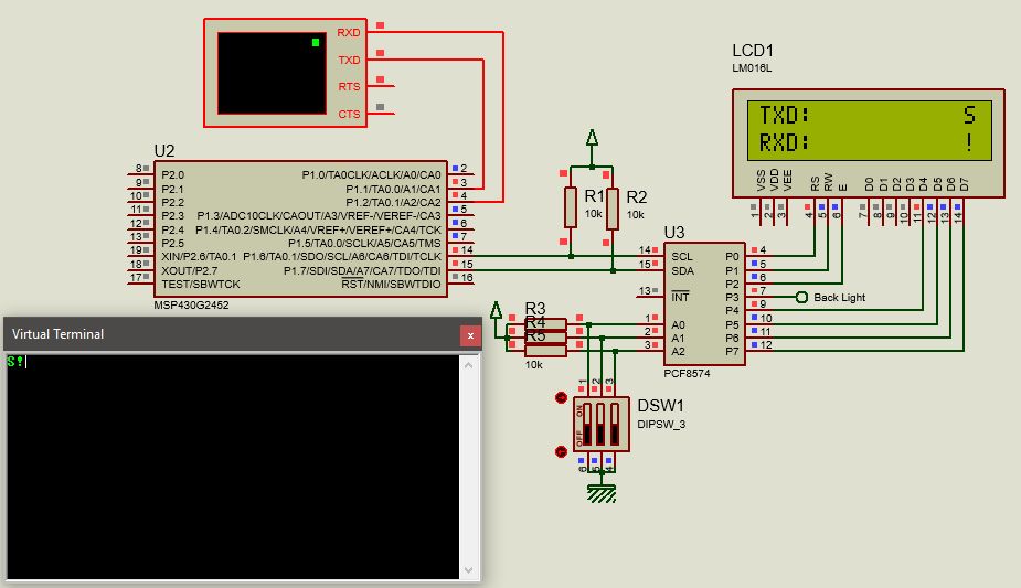
Explanation
Software UART is created with digital I/Os. Thus, the very first task we need to do is to initialize these pins. The SW_UART header file states which pins and ports are used. So, you only need to set these first. All of my codes are modular and so once you set these properly the functions and the definitions associated take care of other tasks. This, in turn, makes the codes easily to use and ready for quick modifications/deployments.
#define SW_UART_RXD_DIR P1DIR
#define SW_UART_TXD_DIR P1DIR
#define SW_UART_RXD_OUT P1OUT
#define SW_UART_TXD_OUT P1OUT
#define SW_UART_RXD_IN P1IN
#define SW_UART_RXD_IN_RES P1REN
#define SW_UART_RXD_PIN BIT1
#define SW_UART_TXD_PIN BIT2
Once the pins are set as per requirement, it is needed to initialize them for software UART functionality.
void SW_UART_init(void)
{
SW_UART_TXD_DIR_OUT();
SW_UART_RXD_DIR_IN();
SW_UART_TXD_OUT_HIGH();
delay_ms(10);
}
The header file also states the communication baud rate and number of bits:
#define baudrate 4800
#define no_of_bits 8
#define one_bit_delay (1000000 / baudrate)
#define half_bit_delay (one_bit_delay / 2)
Based on the baud rate further timing infos are calculated. Software UART is not as reliable as hardware UART and so it is better to use low baud rates. It is even better if it can be skipped. However, when there is no other option or when there is a need for additional UART, it must be used.
The UART transmit and receive functions are written using polling methods. External digital I/O interrupt can be used for receiving data. These functions are created just by studying the signal patterns and using the same tactics as with other software communication libraries. The trick is to emulate/receive the signals as a real hardware would do.
void SW_UART_transmit(unsigned char value)
{
unsigned char bits = 0;
SW_UART_TXD_OUT_LOW();
delay_us(one_bit_delay);
for(bits = 0; bits < no_of_bits; bits++)
{
if((value >> bits) & 0x01)
{
SW_UART_TXD_OUT_HIGH();
}
else
{
SW_UART_TXD_OUT_LOW();
}
delay_us(one_bit_delay);
};
SW_UART_TXD_OUT_HIGH();
delay_us(one_bit_delay);
}
unsigned char SW_UART_receive(void)
{
unsigned char bits = 0;
unsigned char value = 0;
while(SW_UART_RXD_INPUT());
delay_us(one_bit_delay);
delay_us(half_bit_delay);
for(bits = 0; bits < no_of_bits; bits++)
{
if(SW_UART_RXD_INPUT())
{
value += (1 << bits);
}
delay_us(one_bit_delay);
};
if(SW_UART_RXD_INPUT())
{
delay_us(half_bit_delay);
return value;
}
else
{
delay_us(half_bit_delay);
return 0;
}
}
Demo
USCI SPI – Interfacing MPL115A1 Atmospheric Pressure Sensor
We have already seen that MSP430’s USI module can be used to implement both I2C and SPI communication platforms. However, there will be times we will have to use USCI modules. USCI is a bit complicated and is a bit difficult to use in simple terms. Here in this article, however, I kept things simple and projected ways to use this module simply. Four examples of USCI module in I2C and SPI modes will be presented in this article. The first one will demo how to interface a MSP430 device with a MPL115A1 atmospheric pressure sensor in a full-duplex SPI bus. Full-duplex SPI bus is needed the most when interfacing sensors, RTCs, SPI-based memory chips, SD cards, etc.
Code Example
HW_SPI.h
#include <msp430.h>
void HW_SPI_init(void);
void SPI_write(unsigned char tx_data);
unsigned char SPI_read(void);
unsigned char SPI_transfer(unsigned char tx_data);
HW_SPI.c
#include "HW_SPI.h"
void HW_SPI_init(void)
{
UCA0CTL1 |= UCSWRST;
UCA0CTL0 = UCCKPH | UCMSB | UCMST | UCMODE_1 | UCSYNC;
UCA0CTL1 = UCSSEL_2 | UCSWRST;
UCA0BR0 = 8;
UCA0CTL1 &= ~UCSWRST;
}
void SPI_write(unsigned char tx_data)
{
while(!(IFG2 & UCA0TXIFG));
UCA0TXBUF = tx_data;
while(UCA0STAT & UCBUSY);
}
unsigned char SPI_read(void)
{
unsigned char rx_data = 0;
while(!(IFG2 & UCA0RXIFG));
rx_data = UCA0RXBUF;
while(UCA0STAT & UCBUSY);
return rx_data;
}
unsigned char SPI_transfer(unsigned char tx_data)
{
unsigned char rx_data = 0;
while(!(IFG2 & UCA0TXIFG));
UCA0TXBUF = tx_data;
while(UCA0STAT & UCBUSY);
while(!(IFG2 & UCA0RXIFG));
rx_data = UCA0RXBUF;
while(UCA0STAT & UCBUSY);
return rx_data;
}
MPL115A1.h
#include <msp430.h>
#include "delay.h"
#include "HW_SPI.h"
#define LOW 0
#define HIGH 1
#define PRESH 0x80
#define PRESL 0x82
#define TEMPH 0x84
#define TEMPL 0x86
#define A0_H 0x88
#define A0_L 0x8A
#define B1_H 0x8C
#define B1_L 0x8E
#define B2_H 0x90
#define B2_L 0x92
#define C12_H 0x94
#define C12_L 0x96
#define conv_cmd 0x24
#define MPL115A1_CSN_PORT_OUT P2OUT
#define MPL115A1_SDN_PORT_OUT P2OUT
#define MPL115A1_CSN_PORT_DIR P2DIR
#define MPL115A1_SDN_PORT_DIR P2DIR
#define MPL115A1_SDN_pin BIT0
#define MPL115A1_CSN_pin BIT1
#define MPL115A1_SDN_HIGH() P2OUT |= MPL115A1_SDN_pin
#define MPL115A1_SDN_LOW() P2OUT &= ~MPL115A1_SDN_pin
#define MPL115A1_CSN_HIGH() P2OUT |= MPL115A1_CSN_pin
#define MPL115A1_CSN_LOW() P2OUT &= ~MPL115A1_CSN_pin
struct
{
float A0;
float B1;
float B2;
float C12;
}coefficients;
void MPL115A1_init(void);
unsigned char MPL115A1_read(unsigned char address);
void MPL115A1_write(unsigned char address, unsigned char value);
void MPL115A1_get_coefficients(void);
void MPL115A1_get_bytes(unsigned int *hb, unsigned int *lb, unsigned char address);
void MPL115A1_get_data(float *pres, float *temp);
MPL115A1.c
#include "MPL115A1.h"
void MPL115A1_init(void)
{
MPL115A1_SDN_PORT_DIR |= MPL115A1_SDN_pin;
MPL115A1_CSN_PORT_DIR |= MPL115A1_CSN_pin;
MPL115A1_SDN_HIGH();
MPL115A1_CSN_HIGH();
HW_SPI_init();
MPL115A1_get_coefficients();
}
unsigned char MPL115A1_read(unsigned char address)
{
unsigned char value = 0;
MPL115A1_CSN_LOW();
delay_ms(3);
SPI_write(address);
value = SPI_read();
value = SPI_transfer(address);
MPL115A1_CSN_HIGH();
return value;
}
void MPL115A1_write(unsigned char address, unsigned char value)
{
MPL115A1_CSN_LOW();
delay_ms(3);
SPI_write((address & 0x7F));
SPI_write(value);
MPL115A1_CSN_HIGH();
}
void MPL115A1_get_coefficients(void)
{
unsigned int hb = 0;
unsigned int lb = 0;
MPL115A1_get_bytes(&hb, &lb, A0_H);
coefficients.A0 = ((hb << 5) + (lb >> 3) + ((lb & 0x07) / 8.0));
MPL115A1_get_bytes(&hb, &lb, B1_H);
coefficients.B1 = (((((hb & 0x1F) * 0x0100) + lb) / 8192.0) - 3.0);
MPL115A1_get_bytes(&hb, &lb, B2_H);
coefficients.B2 = (((((hb - 0x80) << 8) + lb) / 16384.0) - 2.0);
MPL115A1_get_bytes(&hb, &lb, C12_H);
coefficients.C12 = (((hb * 0x100) + lb) / 16777216.0);
}
void MPL115A1_get_bytes(unsigned int *hb, unsigned int *lb, unsigned char address)
{
*hb = ((unsigned int)MPL115A1_read(address));
*lb = ((unsigned int)MPL115A1_read((address + 2)));
}
void MPL115A1_get_data(float *pres, float *temp)
{
unsigned int hb = 0;
unsigned int lb = 0;
signed long Padc = 0;
signed long Tadc = 0;
MPL115A1_write(conv_cmd, 0);
MPL115A1_get_bytes(&hb, &lb, PRESH);
Padc = (((hb << 8) + lb) >> 6);
MPL115A1_get_bytes(&hb, &lb, TEMPH);
Tadc = (((hb << 8) + lb) >> 6);
*pres = ( coefficients.A0 + (( coefficients.B1 + ( coefficients.C12 * Tadc)) * Padc) + ( coefficients.B2 * Tadc));
*pres = (((*pres * 65.0) / 1023.0) + 50.0);
*temp = (30.0 + ((Tadc - 472) / (-5.35)));
}
main.c
#include <msp430.h>
#include "delay.h"
#include "HW_SPI.h"
#include "SW_I2C.h"
#include "PCF8574.h"
#include "lcd.h"
#include "MPL115A1.h"
const unsigned char symbol[8] =
{
0x00, 0x06, 0x09, 0x09, 0x06, 0x00, 0x00, 0x00
};
void GPIO_graceInit(void);
void BCSplus_graceInit(void);
void USCI_A0_graceInit(void);
void System_graceInit(void);
void WDTplus_graceInit(void);
void lcd_symbol(void);
void print_C(unsigned char x_pos, unsigned char y_pos, signed int value);
void print_I(unsigned char x_pos, unsigned char y_pos, signed long value);
void print_D(unsigned char x_pos, unsigned char y_pos, signed int value, unsigned char points);
void print_F(unsigned char x_pos, unsigned char y_pos, float value, unsigned char points);
void main(void)
{
float t = 0.0;
float p = 0.0;
/* Stop watchdog timer from timing out during initial start-up. */
WDTCTL = WDTPW | WDTHOLD;
/* initialize Config for the MSP430 GPIO */
GPIO_graceInit();
/* initialize Config for the MSP430 2xx family clock systems (BCS) */
BCSplus_graceInit();
/* initialize Config for the MSP430 USCI_A0 */
USCI_A0_graceInit();
/* initialize Config for the MSP430 System Registers */
System_graceInit();
/* initialize Config for the MSP430 WDT+ */
WDTplus_graceInit();
LCD_init();
LCD_clear_home();
lcd_symbol();
LCD_goto(0, 0);
LCD_putstr("P/kPa:");
LCD_goto(0, 1);
LCD_putstr("T/ C :");
LCD_goto(2, 1);
LCD_send(0, DAT);
MPL115A1_init();
while(1)
{
MPL115A1_get_data(&p, &t);
print_F(10, 0, p, 1);
print_F(11, 1, t, 1);
delay_ms(400);
};
}
void GPIO_graceInit(void)
{
/* USER CODE START (section: GPIO_graceInit_prologue) */
/* User initialization code */
/* USER CODE END (section: GPIO_graceInit_prologue) */
/* Port 1 Port Select 2 Register */
P1SEL2 = BIT1 | BIT2 | BIT4;
/* Port 1 Output Register */
P1OUT = 0;
/* Port 1 Port Select Register */
P1SEL = BIT1 | BIT2 | BIT4;
/* Port 1 Direction Register */
P1DIR = 0;
/* Port 1 Interrupt Edge Select Register */
P1IES = 0;
/* Port 1 Interrupt Flag Register */
P1IFG = 0;
/* Port 2 Output Register */
P2OUT = 0;
/* Port 2 Direction Register */
P2DIR = BIT0 | BIT1;
/* Port 2 Interrupt Edge Select Register */
P2IES = 0;
/* Port 2 Interrupt Flag Register */
P2IFG = 0;
/* Port 3 Output Register */
P3OUT = 0;
/* Port 3 Direction Register */
P3DIR = 0;
/* USER CODE START (section: GPIO_graceInit_epilogue) */
/* User code */
/* USER CODE END (section: GPIO_graceInit_epilogue) */
}
void BCSplus_graceInit(void)
{
/* USER CODE START (section: BCSplus_graceInit_prologue) */
/* User initialization code */
/* USER CODE END (section: BCSplus_graceInit_prologue) */
/*
* Basic Clock System Control 2
*
* SELM_0 -- DCOCLK
* DIVM_0 -- Divide by 1
* ~SELS -- DCOCLK
* DIVS_0 -- Divide by 1
* ~DCOR -- DCO uses internal resistor
*
* Note: ~<BIT> indicates that <BIT> has value zero
*/
BCSCTL2 = SELM_0 | DIVM_0 | DIVS_0;
if (CALBC1_8MHZ != 0xFF)
{
/* Adjust this accordingly to your VCC rise time */
__delay_cycles(100000);
// Follow recommended flow. First, clear all DCOx and MODx bits. Then
// apply new RSELx values. Finally, apply new DCOx and MODx bit values.
DCOCTL = 0x00;
BCSCTL1 = CALBC1_8MHZ; /* Set DCO to 8MHz */
DCOCTL = CALDCO_8MHZ;
}
/*
* Basic Clock System Control 1
*
* XT2OFF -- Disable XT2CLK
* ~XTS -- Low Frequency
* DIVA_0 -- Divide by 1
*
* Note: ~XTS indicates that XTS has value zero
*/
BCSCTL1 |= XT2OFF | DIVA_0;
/*
* Basic Clock System Control 3
*
* XT2S_0 -- 0.4 - 1 MHz
* LFXT1S_0 -- If XTS = 0, XT1 = 32768kHz Crystal ; If XTS = 1, XT1 = 0.4 - 1-MHz crystal or resonator
* XCAP_1 -- ~6 pF
*/
BCSCTL3 = XT2S_0 | LFXT1S_0 | XCAP_1;
/* USER CODE START (section: BCSplus_graceInit_epilogue) */
/* User code */
/* USER CODE END (section: BCSplus_graceInit_epilogue) */
}
void USCI_A0_graceInit(void)
{
/* USER CODE START (section: USCI_A0_graceInit_prologue) */
/* User initialization code */
/* USER CODE END (section: USCI_A0_graceInit_prologue) */
/* Disable USCI */
/* Disable USCI */
UCA0CTL1 |= UCSWRST;
/*
* Control Register 0
*
* UCCKPH -- Data is captured on the first UCLK edge and changed on the following edge
* ~UCCKPL -- Inactive state is low
* UCMSB -- MSB first
* ~UC7BIT -- 8-bit
* UCMST -- Master mode
* UCMODE_1 -- 4-Pin SPI with UCxSTE active high: slave enabled when UCxSTE = 1
* UCSYNC -- Synchronous Mode
*
* Note: ~<BIT> indicates that <BIT> has value zero
*/
UCA0CTL0 = UCCKPH | UCMSB | UCMST | UCMODE_1 | UCSYNC;
/*
* Control Register 1
*
* UCSSEL_2 -- SMCLK
* UCSWRST -- Enabled. USCI logic held in reset state
*/
UCA0CTL1 = UCSSEL_2 | UCSWRST;
/* Bit Rate Control Register 0 */
UCA0BR0 = 8;
/* Enable USCI */
UCA0CTL1 &= ~UCSWRST;
/* USER CODE START (section: USCI_A0_graceInit_epilogue) */
/* User code */
/* USER CODE END (section: USCI_A0_graceInit_epilogue) */
}
void System_graceInit(void)
{
/* USER CODE START (section: System_graceInit_prologue) */
/* User initialization code */
/* USER CODE END (section: System_graceInit_prologue) */
/*
* SR, Status Register
*
* ~SCG1 -- Disable System clock generator 1
* ~SCG0 -- Disable System clock generator 0
* ~OSCOFF -- Oscillator On
* ~CPUOFF -- CPU On
* GIE -- General interrupt enable
*
* Note: ~<BIT> indicates that <BIT> has value zero
*/
__bis_SR_register(GIE);
/* USER CODE START (section: System_graceInit_epilogue) */
/* User code */
/* USER CODE END (section: System_graceInit_epilogue) */
}
void WDTplus_graceInit(void)
{
/* USER CODE START (section: RTC_B_graceInit_prologue) */
/* User initialization code */
/* USER CODE END (section: RTC_B_graceInit_prologue) */
/*
* WDTCTL, Watchdog Timer+ Register
*
* WDTPW -- Watchdog password
* WDTHOLD -- Watchdog timer+ is stopped
* ~WDTNMIES -- NMI on rising edge
* ~WDTNMI -- Reset function
* ~WDTTMSEL -- Watchdog mode
* ~WDTCNTCL -- No action
* ~WDTSSEL -- SMCLK
* ~WDTIS0 -- Watchdog clock source bit0 disabled
* ~WDTIS1 -- Watchdog clock source bit1 disabled
*
* Note: ~<BIT> indicates that <BIT> has value zero
*/
WDTCTL = WDTPW | WDTHOLD;
/* USER CODE START (section: RTC_B_graceInit_epilogue) */
/* User code */
/* USER CODE END (section: RTC_B_graceInit_epilogue) */
}
void lcd_symbol(void)
{
unsigned char s = 0;
LCD_send(0x40, CMD);
for(s = 0; s < 8; s++)
{
LCD_send(symbol[s], DAT);
}
LCD_send(0x80, CMD);
}
void print_C(unsigned char x_pos, unsigned char y_pos, signed int value)
{
char ch[5] = {0x20, 0x20, 0x20, 0x20, '\0'};
if(value < 0x00)
{
ch[0] = 0x2D;
value = -value;
}
else
{
ch[0] = 0x20;
}
if((value > 99) && (value <= 999))
{
ch[1] = ((value / 100) + 0x30);
ch[2] = (((value % 100) / 10) + 0x30);
ch[3] = ((value % 10) + 0x30);
}
else if((value > 9) && (value <= 99))
{
ch[1] = (((value % 100) / 10) + 0x30);
ch[2] = ((value % 10) + 0x30);
ch[3] = 0x20;
}
else if((value >= 0) && (value <= 9))
{
ch[1] = ((value % 10) + 0x30);
ch[2] = 0x20;
ch[3] = 0x20;
}
LCD_goto(x_pos, y_pos);
LCD_putstr(ch);
}
void print_I(unsigned char x_pos, unsigned char y_pos, signed long value)
{
char ch[7] = {0x20, 0x20, 0x20, 0x20, 0x20, 0x20, '\0'};
if(value < 0)
{
ch[0] = 0x2D;
value = -value;
}
else
{
ch[0] = 0x20;
}
if(value > 9999)
{
ch[1] = ((value / 10000) + 0x30);
ch[2] = (((value % 10000)/ 1000) + 0x30);
ch[3] = (((value % 1000) / 100) + 0x30);
ch[4] = (((value % 100) / 10) + 0x30);
ch[5] = ((value % 10) + 0x30);
}
else if((value > 999) && (value <= 9999))
{
ch[1] = (((value % 10000)/ 1000) + 0x30);
ch[2] = (((value % 1000) / 100) + 0x30);
ch[3] = (((value % 100) / 10) + 0x30);
ch[4] = ((value % 10) + 0x30);
ch[5] = 0x20;
}
else if((value > 99) && (value <= 999))
{
ch[1] = (((value % 1000) / 100) + 0x30);
ch[2] = (((value % 100) / 10) + 0x30);
ch[3] = ((value % 10) + 0x30);
ch[4] = 0x20;
ch[5] = 0x20;
}
else if((value > 9) && (value <= 99))
{
ch[1] = (((value % 100) / 10) + 0x30);
ch[2] = ((value % 10) + 0x30);
ch[3] = 0x20;
ch[4] = 0x20;
ch[5] = 0x20;
}
else
{
ch[1] = ((value % 10) + 0x30);
ch[2] = 0x20;
ch[3] = 0x20;
ch[4] = 0x20;
ch[5] = 0x20;
}
LCD_goto(x_pos, y_pos);
LCD_putstr(ch);
}
void print_D(unsigned char x_pos, unsigned char y_pos, signed int value, unsigned char points)
{
char ch[5] = {0x2E, 0x20, 0x20, '\0'};
ch[1] = ((value / 100) + 0x30);
if(points > 1)
{
ch[2] = (((value / 10) % 10) + 0x30);
if(points > 1)
{
ch[3] = ((value % 10) + 0x30);
}
}
LCD_goto(x_pos, y_pos);
LCD_putstr(ch);
}
void print_F(unsigned char x_pos, unsigned char y_pos, float value, unsigned char points)
{
signed long tmp = 0x0000;
tmp = value;
print_I(x_pos, y_pos, tmp);
tmp = ((value - tmp) * 1000);
if(tmp < 0)
{
tmp = -tmp;
}
if(value < 0)
{
value = -value;
LCD_goto(x_pos, y_pos);
LCD_putchar(0x2D);
}
else
{
LCD_goto(x_pos, y_pos);
LCD_putchar(0x20);
}
if((value >= 10000) && (value < 100000))
{
print_D((x_pos + 6), y_pos, tmp, points);
}
else if((value >= 1000) && (value < 10000))
{
print_D((x_pos + 5), y_pos, tmp, points);
}
else if((value >= 100) && (value < 1000))
{
print_D((x_pos + 4), y_pos, tmp, points);
}
else if((value >= 10) && (value < 100))
{
print_D((x_pos + 3), y_pos, tmp, points);
}
else if(value < 10)
{
print_D((x_pos + 2), y_pos, tmp, points);
}
}
Simulation
The model for MPL115A1 is not available in Proteus VSM and so it cannot be simulated. Only the pinouts are shown in the schematic below.

Explanation
HW_SPI.h and HW_SPI.c files describe the functionality of USCI-SPI hardware.
void HW_SPI_init(void);
void SPI_write(unsigned char tx_data);
unsigned char SPI_read(void);
unsigned char SPI_transfer(unsigned char tx_data);
The first function as shown above initiates the USCI-SPI hardware. The initialization is generated using Grace. Note the Grace screenshot below:
These settings describe which pins are being used, their purposes, communication speed, SPI mode, clock polarity and so on. Note the slave select pin is not shown here as we have used a different pin for that purpose.
SPI_read, SPI_write and SPI_transfer functions do their jobs as per their namings.
Now let’s get inside the read and write function of USCI-SPI
void SPI_write(unsigned char tx_data)
{
while(!(IFG2 & UCA0TXIFG));
UCA0TXBUF = tx_data;
while(UCA0STAT & UCBUSY);
}
unsigned char SPI_read(void)
{
unsigned char rx_data = 0;
while(!(IFG2 & UCA0RXIFG));
rx_data = UCA0RXBUF;
while(UCA0STAT & UCBUSY);
return rx_data;
}
unsigned char SPI_transfer(unsigned char tx_data)
{
unsigned char rx_data = 0;
while(!(IFG2 & UCA0TXIFG));
UCA0TXBUF = tx_data;
while(UCA0STAT & UCBUSY);
while(!(IFG2 & UCA0RXIFG));
rx_data = UCA0RXBUF;
while(UCA0STAT & UCBUSY);
return rx_data;
}
The SPI read and write processes are simplest to understand. Before starting communication, respective data transaction interrupt flags are polled. Note that these flags are needed even if we don’t use USCI interrupts. Once polled okay, data is sent from MSP430 device in SPI write mode or received while in read mode. Then we have to check if data has been fully received/transmitted by asserting the USCI busy flag. Lastly the USCI SPI transfer function is a mixture of both SPI read and write functions.
The code here is used to read a MPL115A1 barometric pressure sensor and display atmospheric pressure-temperature data. MPL115A1 uses full-duplex SPI communication medium to communicate with its host device and here MSP430’s USCI_A0 in SPI mode is employed to achieved that.
Demo

USCI SPI – Interfacing SSD1306 OLED Display
SPI is perhaps best known for the communication speed it offers. This raw communication speed is most needed when we need to interface external memories and smart displays like TFT displays and OLED displays. Here, we will see how to interface a SSD1306 OLED display with MSP430 using half-duplex or unidirectional USCI-based SPI communication bus.
Code Example
HW_SPI.h
#include <msp430.h>
void HW_SPI_init(void);
void SPI_write(unsigned char tx_data);
unsigned char SPI_read(void);
unsigned char SPI_transfer(unsigned char tx_data);
HW_SPI.c
#include "HW_SPI.h"
void HW_SPI_init(void)
{
UCB0CTL1 |= UCSWRST;
UCB0CTL0 = UCCKPH | UCMSB | UCMST | UCMODE_1 | UCSYNC;
UCB0CTL1 = UCSSEL_2;
UCB0BR0 = 8;
UCB0BR1 = 0;
UCB0CTL1 &= ~UCSWRST;
}
void SPI_write(unsigned char tx_data)
{
while(!(IFG2 & UCB0TXIFG));
UCB0TXBUF = tx_data;
while(UCB0STAT & UCBUSY);
}
unsigned char SPI_read(void)
{
unsigned char rx_data = 0;
while(!(IFG2 & UCB0RXIFG));
rx_data = UCB0RXBUF;
while(UCB0STAT & UCBUSY);
return rx_data;
}
unsigned char SPI_transfer(unsigned char tx_data)
{
unsigned char rx_data = 0;
while(!(IFG2 & UCB0TXIFG));
UCB0TXBUF = tx_data;
while(UCB0STAT & UCBUSY);
while(!(IFG2 & UCB0RXIFG));
rx_data = UCB0RXBUF;
while(UCB0STAT & UCBUSY);
return rx_data;
}
SSD1306.h
#include <MSP430.h>
#include "delay.h"
#include "HW_SPI.h"
#define OLED_PORT P1OUT
#define OLED_DIR P1DIR
#define RST_pin BIT2
#define DC_pin BIT3
#define CS_pin BIT4
#define OLED_PORT_OUT() OLED_DIR |= (RST_pin | DC_pin | CS_pin)
#define OLED_RST_HIGH() OLED_PORT |= RST_pin
#define OLED_RST_LOW() OLED_PORT &= ~RST_pin
#define OLED_DC_HIGH() OLED_PORT |= DC_pin
#define OLED_DC_LOW() OLED_PORT &= ~DC_pin
#define OLED_CS_HIGH() OLED_PORT |= CS_pin
#define OLED_CS_LOW() OLED_PORT &= ~CS_pin
#define Set_Lower_Column_Start_Address_CMD 0x00
#define Set_Higher_Column_Start_Address_CMD 0x10
#define Set_Memory_Addressing_Mode_CMD 0x20
#define Set_Column_Address_CMD 0x21
#define Set_Page_Address_CMD 0x22
#define Set_Display_Start_Line_CMD 0x40
#define Set_Contrast_Control_CMD 0x81
#define Set_Charge_Pump_CMD 0x8D
#define Set_Segment_Remap_CMD 0xA0
#define Set_Entire_Display_ON_CMD 0xA4
#define Set_Normal_or_Inverse_Display_CMD 0xA6
#define Set_Multiplex_Ratio_CMD 0xA8
#define Set_Display_ON_or_OFF_CMD 0xAE
#define Set_Page_Start_Address_CMD 0xB0
#define Set_COM_Output_Scan_Direction_CMD 0xC0
#define Set_Display_Offset_CMD 0xD3
#define Set_Display_Clock_CMD 0xD5
#define Set_Pre_charge_Period_CMD 0xD9
#define Set_Common_HW_Config_CMD 0xDA
#define Set_VCOMH_Level_CMD 0xDB
#define Set_NOP_CMD 0xE3
#define Horizontal_Addressing_Mode 0x00
#define Vertical_Addressing_Mode 0x01
#define Page_Addressing_Mode 0x02
#define Disable_Charge_Pump 0x00
#define Enable_Charge_Pump 0x04
#define Column_Address_0_Mapped_to_SEG0 0x00
#define Column_Address_0_Mapped_to_SEG127 0x01
#define Normal_Display 0x00
#define Entire_Display_ON 0x01
#define Non_Inverted_Display 0x00
#define Inverted_Display 0x01
#define Display_OFF 0x00
#define Display_ON 0x01
#define Scan_from_COM0_to_63 0x00
#define Scan_from_COM63_to_0 0x08
#define x_size 128
#define x_max x_size
#define x_min 0
#define y_size 64
#define y_max 8
#define y_min 0
#define ON 1
#define OFF 0
#define YES 1
#define NO 0
#define HIGH 1
#define LOW 0
#define DAT 1
#define CMD 0
void setup_GPIOs(void);
void OLED_init(void);
void OLED_reset_sequence(void);
void OLED_write(unsigned char value, unsigned char type);
void OLED_gotoxy(unsigned char x_pos, unsigned char y_pos);
void OLED_fill(unsigned char bmp_data);
void OLED_clear_screen(void);
void OLED_cursor(unsigned char x_pos, unsigned char y_pos);
void OLED_print_char(unsigned char x_pos, unsigned char y_pos, unsigned char ch);
void OLED_print_string(unsigned char x_pos, unsigned char y_pos, unsigned char *ch);
void OLED_print_chr(unsigned char x_pos, unsigned char y_pos, signed int value);
void OLED_print_int(unsigned char x_pos, unsigned char y_pos, signed long value);
void OLED_print_decimal(unsigned char x_pos, unsigned char y_pos, unsigned int value, unsigned char points);
void OLED_print_float(unsigned char x_pos, unsigned char y_pos, float value, unsigned char points);
SSD1306.c
#include "SSD1306.h"
#include "fonts.h"
void setup_GPIOs(void)
{
OLED_PORT_OUT();
P1SEL2 = BIT5 | BIT7;
P1SEL = BIT5 | BIT7;
}
void OLED_init(void)
{
setup_GPIOs();
HW_SPI_init();
OLED_reset_sequence();
OLED_write((Set_Display_ON_or_OFF_CMD + Display_OFF), CMD);
OLED_write(Set_Display_Clock_CMD, CMD);
OLED_write(0x80, CMD);
OLED_write(Set_Multiplex_Ratio_CMD, CMD);
OLED_write(0x3F, CMD);
OLED_write(Set_Display_Offset_CMD, CMD);
OLED_write(0x00, CMD);
OLED_write((Set_Display_Start_Line_CMD | 0x00), CMD);
OLED_write(Set_Charge_Pump_CMD, CMD);
OLED_write((Set_Higher_Column_Start_Address_CMD | Enable_Charge_Pump), CMD);
OLED_write(Set_Memory_Addressing_Mode_CMD, CMD);
OLED_write(Page_Addressing_Mode, CMD);
OLED_write((Set_Segment_Remap_CMD | Column_Address_0_Mapped_to_SEG127), CMD);
OLED_write((Set_COM_Output_Scan_Direction_CMD | Scan_from_COM63_to_0), CMD);
OLED_write(Set_Common_HW_Config_CMD, CMD);
OLED_write(0x12, CMD);
OLED_write(Set_Contrast_Control_CMD, CMD);
OLED_write(0xCF, CMD);
OLED_write(Set_Pre_charge_Period_CMD, CMD);
OLED_write(0xF1, CMD);
OLED_write(Set_VCOMH_Level_CMD, CMD);
OLED_write(0x40, CMD);
OLED_write((Set_Entire_Display_ON_CMD | Normal_Display), CMD);
OLED_write((Set_Normal_or_Inverse_Display_CMD | Non_Inverted_Display), CMD);
OLED_write((Set_Display_ON_or_OFF_CMD + Display_ON) , CMD);
OLED_gotoxy(0, 0);
OLED_clear_screen();
}
void OLED_reset_sequence(void)
{
delay_ms(40);
OLED_RST_LOW();
delay_ms(40);
OLED_RST_HIGH();
}
void OLED_write(unsigned char value, unsigned char type)
{
switch(type)
{
case DAT:
{
OLED_DC_HIGH();
break;
}
case CMD:
{
OLED_DC_LOW();
break;
}
}
OLED_CS_LOW();
SPI_transfer(value);
OLED_CS_HIGH();
}
void OLED_gotoxy(unsigned char x_pos, unsigned char y_pos)
{
OLED_write((Set_Page_Start_Address_CMD + y_pos), CMD);
OLED_write(((x_pos & 0x0F) | Set_Lower_Column_Start_Address_CMD), CMD);
OLED_write((((x_pos & 0xF0) >> 0x04) | Set_Higher_Column_Start_Address_CMD), CMD);
}
void OLED_fill(unsigned char bmp_data)
{
unsigned char x_pos = 0;
unsigned char page = 0;
for(page = y_min; page < y_max; page++)
{
OLED_write((Set_Page_Start_Address_CMD + page), CMD);
OLED_write(Set_Lower_Column_Start_Address_CMD, CMD);
OLED_write(Set_Higher_Column_Start_Address_CMD, CMD);
for(x_pos = x_min; x_pos < x_max; x_pos++)
{
OLED_write(bmp_data, DAT);
}
}
}
void OLED_clear_screen(void)
{
OLED_fill(0x00);
}
void OLED_cursor(unsigned char x_pos, unsigned char y_pos)
{
unsigned char i = 0;
if(y_pos != 0)
{
if(x_pos == 1)
{
OLED_gotoxy(0x00, (y_pos + 0x02));
}
else
{
OLED_gotoxy((0x50 + ((x_pos - 0x02) * 0x06)), (y_pos + 0x02));
}
for(i = 0; i < 6; i++)
{
OLED_write(0xFF, DAT);
}
}
}
void OLED_print_char(unsigned char x_pos, unsigned char y_pos, unsigned char ch)
{
unsigned char chr = 0;
unsigned char s = 0;
chr = (ch - 32);
if(x_pos > (x_max - 6))
{
x_pos = 0;
y_pos++;
}
OLED_gotoxy(x_pos, y_pos);
for(s = 0; s < 6; s++)
{
OLED_write(font_regular[chr][s], DAT);
}
}
void OLED_print_string(unsigned char x_pos, unsigned char y_pos, unsigned char *ch)
{
unsigned char chr = 0;
unsigned char i = 0;
unsigned char j = 0;
while(ch[j] != '\0')
{
chr = (ch[j] - 32);
if(x_pos > (x_max - 0x06))
{
x_pos = 0x00;
y_pos++;
}
OLED_gotoxy(x_pos, y_pos);
for(i = 0; i < 6; i++)
{
OLED_write(font_regular[chr][i], DAT);
}
j++;
x_pos += 6;
}
}
void OLED_print_chr(unsigned char x_pos, unsigned char y_pos, signed int value)
{
unsigned char ch = 0;
if(value < 0)
{
OLED_print_char(x_pos, y_pos, '-');
value = -value;
}
else
{
OLED_print_char(x_pos, y_pos,' ');
}
if((value > 99) && (value <= 999))
{
ch = (value / 100);
OLED_print_char((x_pos + 6), y_pos , (0x30 + ch));
ch = ((value % 100) / 10);
OLED_print_char((x_pos + 12), y_pos , (0x30 + ch));
ch = (value % 10);
OLED_print_char((x_pos + 18), y_pos , (0x30 + ch));
}
else if((value > 9) && (value <= 99))
{
ch = ((value % 100) / 10);
OLED_print_char((x_pos + 6), y_pos , (0x30 + ch));
ch = (value % 10);
OLED_print_char((x_pos + 12), y_pos , (0x30 + ch));
OLED_print_char((x_pos + 18), y_pos , 0x20);
}
else if((value >= 0) && (value <= 9))
{
ch = (value % 10);
OLED_print_char((x_pos + 6), y_pos , (0x30 + ch));
OLED_print_char((x_pos + 12), y_pos , 0x20);
OLED_print_char((x_pos + 18), y_pos , 0x20);
}
}
void OLED_print_int(unsigned char x_pos, unsigned char y_pos, signed long value)
{
unsigned char ch = 0;
if(value < 0)
{
OLED_print_char(x_pos, y_pos, '-');
value = -value;
}
else
{
OLED_print_char(x_pos, y_pos,' ');
}
if(value > 9999)
{
ch = (value / 10000);
OLED_print_char((x_pos + 6), y_pos , (0x30 + ch));
ch = ((value % 10000)/ 1000);
OLED_print_char((x_pos + 12), y_pos , (0x30 + ch));
ch = ((value % 1000) / 100);
OLED_print_char((x_pos + 18), y_pos , (0x30 + ch));
ch = ((value % 100) / 10);
OLED_print_char((x_pos + 24), y_pos , (0x30 + ch));
ch = (value % 10);
OLED_print_char((x_pos + 30), y_pos , (0x30 + ch));
}
else if((value > 999) && (value <= 9999))
{
ch = ((value % 10000)/ 1000);
OLED_print_char((x_pos + 6), y_pos , (0x30 + ch));
ch = ((value % 1000) / 100);
OLED_print_char((x_pos + 12), y_pos , (0x30 + ch));
ch = ((value % 100) / 10);
OLED_print_char((x_pos + 18), y_pos , (0x30 + ch));
ch = (value % 10);
OLED_print_char((x_pos + 24), y_pos , (0x30 + ch));
OLED_print_char((x_pos + 30), y_pos , 0x20);
}
else if((value > 99) && (value <= 999))
{
ch = ((value % 1000) / 100);
OLED_print_char((x_pos + 6), y_pos , (0x30 + ch));
ch = ((value % 100) / 10);
OLED_print_char((x_pos + 12), y_pos , (0x30 + ch));
ch = (value % 10);
OLED_print_char((x_pos + 18), y_pos , (0x30 + ch));
OLED_print_char((x_pos + 24), y_pos , 0x20);
OLED_print_char((x_pos + 30), y_pos , 0x20);
}
else if((value > 9) && (value <= 99))
{
ch = ((value % 100) / 10);
OLED_print_char((x_pos + 6), y_pos , (0x30 + ch));
ch = (value % 10);
OLED_print_char((x_pos + 12), y_pos , (0x30 + ch));
OLED_print_char((x_pos + 18), y_pos , 0x20);
OLED_print_char((x_pos + 24), y_pos , 0x20);
OLED_print_char((x_pos + 30), y_pos , 0x20);
}
else
{
ch = (value % 10);
OLED_print_char((x_pos + 6), y_pos , (0x30 + ch));
OLED_print_char((x_pos + 12), y_pos , 0x20);
OLED_print_char((x_pos + 18), y_pos , 0x20);
OLED_print_char((x_pos + 24), y_pos , 0x20);
OLED_print_char((x_pos + 30), y_pos , 0x20);
}
}
void OLED_print_decimal(unsigned char x_pos, unsigned char y_pos, unsigned int value, unsigned char points)
{
unsigned char ch = 0;
OLED_print_char(x_pos, y_pos, '.');
ch = (value / 1000);
OLED_print_char((x_pos + 6), y_pos , (0x30 + ch));
if(points > 1)
{
ch = ((value % 1000) / 100);
OLED_print_char((x_pos + 12), y_pos , (0x30 + ch));
if(points > 2)
{
ch = ((value % 100) / 10);
OLED_print_char((x_pos + 18), y_pos , (0x30 + ch));
if(points > 3)
{
ch = (value % 10);
OLED_print_char((x_pos + 24), y_pos , (0x30 + ch));
}
}
}
}
void OLED_print_float(unsigned char x_pos, unsigned char y_pos, float value, unsigned char points)
{
signed long tmp = 0;
tmp = value;
OLED_print_int(x_pos, y_pos, tmp);
tmp = ((value - tmp) * 10000);
if(tmp < 0)
{
tmp = -tmp;
}
if((value >= 10000) && (value < 100000))
{
OLED_print_decimal((x_pos + 36), y_pos, tmp, points);
}
else if((value >= 1000) && (value < 10000))
{
OLED_print_decimal((x_pos + 30), y_pos, tmp, points);
}
else if((value >= 100) && (value < 1000))
{
OLED_print_decimal((x_pos + 24), y_pos, tmp, points);
}
else if((value >= 10) && (value < 100))
{
OLED_print_decimal((x_pos + 18), y_pos, tmp, points);
}
else if(value < 10)
{
OLED_print_decimal((x_pos + 12), y_pos, tmp, points);
if(value < 0)
{
OLED_print_char(x_pos, y_pos, '-');
}
else
{
OLED_print_char(x_pos, y_pos, ' ');
}
}
}
main.c
#include <msp430.h>
#include "delay.h"
#include "HW_SPI.h"
#include "SSD1306.h"
void GPIO_graceInit(void);
void BCSplus_graceInit(void);
void USCI_B0_graceInit(void);
void System_graceInit(void);
void WDTplus_graceInit(void);
void main(void)
{
signed char c = -11;
signed int i = -111;
float f = -1.9;
/* Stop watchdog timer from timing out during initial start-up. */
WDTCTL = WDTPW | WDTHOLD;
/* initialize Config for the MSP430 GPIO */
GPIO_graceInit();
/* initialize Config for the MSP430 2xx family clock systems (BCS) */
BCSplus_graceInit();
/* initialize Config for the MSP430 USCI_B0 */
USCI_B0_graceInit();
/* initialize Config for the MSP430 System Registers */
System_graceInit();
/* initialize Config for the MSP430 WDT+ */
WDTplus_graceInit();
OLED_init();
OLED_print_string(4, 0, "MSP430G2553 SSD1306");
OLED_print_string(16, 1, "USCI_B0 SPI Test");
OLED_print_string(0, 4, "Char :");
OLED_print_string(0, 5, "Int. :");
OLED_print_string(0, 6, "Float:");
while(1)
{
OLED_print_chr(92, 4, c);
OLED_print_int(92, 5, i);
OLED_print_float(92, 6, f, 1);
c++;
i++;
f += 0.1;
delay_ms(200);
};
}
void GPIO_graceInit(void)
{
/* USER CODE START (section: GPIO_graceInit_prologue) */
/* User initialization code */
/* USER CODE END (section: GPIO_graceInit_prologue) */
/* Port 1 Port Select 2 Register */
P1SEL2 = BIT5 | BIT7;
/* Port 1 Output Register */
P1OUT = 0;
/* Port 1 Port Select Register */
P1SEL = BIT5 | BIT7;
/* Port 1 Direction Register */
P1DIR = BIT2 | BIT3 | BIT4;
/* Port 1 Interrupt Edge Select Register */
P1IES = 0;
/* Port 1 Interrupt Flag Register */
P1IFG = 0;
/* Port 2 Output Register */
P2OUT = 0;
/* Port 2 Direction Register */
P2DIR = 0;
/* Port 2 Interrupt Edge Select Register */
P2IES = 0;
/* Port 2 Interrupt Flag Register */
P2IFG = 0;
/* Port 3 Output Register */
P3OUT = 0;
/* Port 3 Direction Register */
P3DIR = 0;
/* USER CODE START (section: GPIO_graceInit_epilogue) */
/* User code */
/* USER CODE END (section: GPIO_graceInit_epilogue) */
}
void BCSplus_graceInit(void)
{
/* USER CODE START (section: BCSplus_graceInit_prologue) */
/* User initialization code */
/* USER CODE END (section: BCSplus_graceInit_prologue) */
/*
* Basic Clock System Control 2
*
* SELM_0 -- DCOCLK
* DIVM_0 -- Divide by 1
* ~SELS -- DCOCLK
* DIVS_0 -- Divide by 1
* ~DCOR -- DCO uses internal resistor
*
* Note: ~<BIT> indicates that <BIT> has value zero
*/
BCSCTL2 = SELM_0 | DIVM_0 | DIVS_0;
if (CALBC1_8MHZ != 0xFF)
{
/* Adjust this accordingly to your VCC rise time */
__delay_cycles(100000);
// Follow recommended flow. First, clear all DCOx and MODx bits. Then
// apply new RSELx values. Finally, apply new DCOx and MODx bit values.
DCOCTL = 0x00;
BCSCTL1 = CALBC1_8MHZ; /* Set DCO to 8MHz */
DCOCTL = CALDCO_8MHZ;
}
/*
* Basic Clock System Control 1
*
* XT2OFF -- Disable XT2CLK
* ~XTS -- Low Frequency
* DIVA_0 -- Divide by 1
*
* Note: ~XTS indicates that XTS has value zero
*/
BCSCTL1 |= XT2OFF | DIVA_0;
/*
* Basic Clock System Control 3
*
* XT2S_0 -- 0.4 - 1 MHz
* LFXT1S_0 -- If XTS = 0, XT1 = 32768kHz Crystal ; If XTS = 1, XT1 = 0.4 - 1-MHz crystal or resonator
* XCAP_1 -- ~6 pF
*/
BCSCTL3 = XT2S_0 | LFXT1S_0 | XCAP_1;
/* USER CODE START (section: BCSplus_graceInit_epilogue) */
/* User code */
/* USER CODE END (section: BCSplus_graceInit_epilogue) */
}
void USCI_B0_graceInit(void)
{
/* USER CODE START (section: USCI_B0_graceInit_prologue) */
/* User initialization code */
/* USER CODE END (section: USCI_B0_graceInit_prologue) */
/* Disable USCI */
UCB0CTL1 |= UCSWRST;
/*
* Control Register 0
*
* UCCKPH -- Data is captured on the first UCLK edge and changed on the following edge
* ~UCCKPL -- Inactive state is low
* UCMSB -- MSB first
* ~UC7BIT -- 8-bit
* UCMST -- Master mode
* UCMODE_1 -- 4-Pin SPI with UCxSTE active high: slave enabled when UCxSTE = 1
* UCSYNC -- Synchronous Mode
*
* Note: ~<BIT> indicates that <BIT> has value zero
*/
UCB0CTL0 = UCCKPH | UCMSB | UCMST | UCMODE_1 | UCSYNC;
/*
* Control Register 1
*
* UCSSEL_2 -- SMCLK
* UCSWRST -- Enabled. USCI logic held in reset state
*/
UCB0CTL1 = UCSSEL_2 | UCSWRST;
/* Bit Rate Control Register 0 */
UCB0BR0 = 8;
/* Enable USCI */
UCB0CTL1 &= ~UCSWRST;
/* USER CODE START (section: USCI_B0_graceInit_epilogue) */
/* User code */
/* USER CODE END (section: USCI_B0_graceInit_epilogue) */
}
void System_graceInit(void)
{
/* USER CODE START (section: System_graceInit_prologue) */
/* User initialization code */
/* USER CODE END (section: System_graceInit_prologue) */
/*
* SR, Status Register
*
* ~SCG1 -- Disable System clock generator 1
* ~SCG0 -- Disable System clock generator 0
* ~OSCOFF -- Oscillator On
* ~CPUOFF -- CPU On
* GIE -- General interrupt enable
*
* Note: ~<BIT> indicates that <BIT> has value zero
*/
__bis_SR_register(GIE);
/* USER CODE START (section: System_graceInit_epilogue) */
/* User code */
/* USER CODE END (section: System_graceInit_epilogue) */
}
void WDTplus_graceInit(void)
{
/* USER CODE START (section: RTC_B_graceInit_prologue) */
/* User initialization code */
/* USER CODE END (section: RTC_B_graceInit_prologue) */
/*
* WDTCTL, Watchdog Timer+ Register
*
* WDTPW -- Watchdog password
* WDTHOLD -- Watchdog timer+ is stopped
* ~WDTNMIES -- NMI on rising edge
* ~WDTNMI -- Reset function
* ~WDTTMSEL -- Watchdog mode
* ~WDTCNTCL -- No action
* ~WDTSSEL -- SMCLK
* ~WDTIS0 -- Watchdog clock source bit0 disabled
* ~WDTIS1 -- Watchdog clock source bit1 disabled
*
* Note: ~<BIT> indicates that <BIT> has value zero
*/
WDTCTL = WDTPW | WDTHOLD;
/* USER CODE START (section: RTC_B_graceInit_epilogue) */
/* User code */
/* USER CODE END (section: RTC_B_graceInit_epilogue) */
}
Simulation
The model for SPI-based SSD1306 OLED display is not available in Proteus VSM and so it cannot be simulated. Only the pinouts are shown in the schematic below.
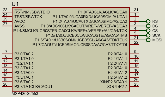
Explanation
The code here basically uses the same functions as in the previous example except for the fact that USCI_B0 is used in half-duplex mode here. The rest of the code is the driver implementation for SSD1306 OLED display. Note that the driver has been cut short of graphical functions due to low memory capacity of Value-Line Devices. Explaining the operation of the OLED display is beyond the scope of this article.
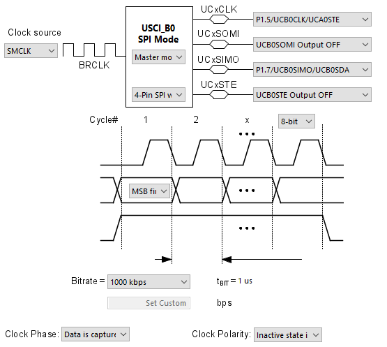
Demo
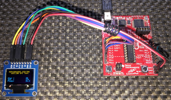
USCI I2C – Interfacing BH1750 Ambient Light Sensor
Using USCI in I2C mode is a bit difficult compared to using USCI in SPI mode. This is because of the many iterations and function calls in I2C mode. Again, here I tried to keep things simple and kept things in a fashion we would normally expect. USCI-based I2C can be realized with a state-of-machine too but that way is not easy for beginners.
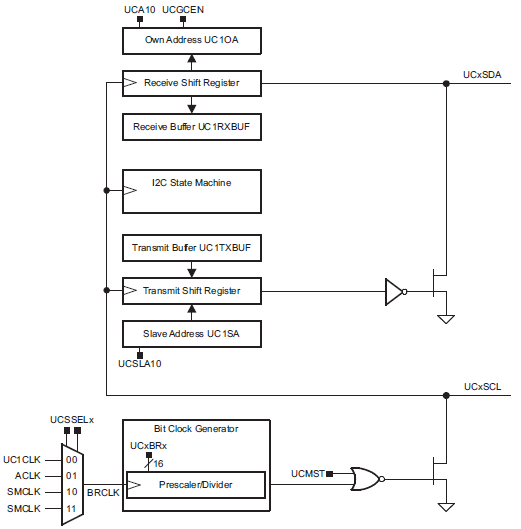
Code Example
HW_I2C.h
#include <msp430.h>
void I2C_USCI_init(unsigned char address);
void I2C_USCI_set_address(unsigned char address);
unsigned char I2C_USCI_read_byte(unsigned char address);
unsigned char I2C_USCI_read_word(unsigned char address,unsigned char *value, unsigned char length);
unsigned char I2C_USCI_write_byte(unsigned char address, unsigned char value);
HW_I2C.c
#include "HW_I2C.h"
void I2C_USCI_init(unsigned char address)
{
P1DIR &= ~(BIT6 + BIT7);
P1OUT |= (BIT6 + BIT7);
P1SEL2 |= (BIT6 | BIT7);
P1SEL |= (BIT6 | BIT7);
UCB0CTL1 |= UCSWRST;
UCB0CTL0 = (UCMST | UCMODE_3 | UCSYNC);
UCB0CTL1 = (UCSSEL_2 | UCSWRST);
UCB0BR0 = 20;
UCB0I2CSA = address;
UCB0CTL1 &= ~UCSWRST;
}
void I2C_USCI_set_address(unsigned char address)
{
UCB0CTL1 |= UCSWRST;
UCB0I2CSA = address;
UCB0CTL1 &= ~UCSWRST;
}
unsigned char I2C_USCI_read_byte(unsigned char address)
{
while(UCB0CTL1 & UCTXSTP);
UCB0CTL1 |= (UCTR | UCTXSTT);
while(!(IFG2 & UCB0TXIFG));
UCB0TXBUF = address;
while(!(IFG2 & UCB0TXIFG));
UCB0CTL1 &= ~UCTR;
UCB0CTL1 |= UCTXSTT;
IFG2 &= ~UCB0TXIFG;
while(UCB0CTL1 & UCTXSTT);
UCB0CTL1 |= UCTXSTP;
return UCB0RXBUF;
}
unsigned char I2C_USCI_read_word(unsigned char address,unsigned char *value, unsigned char length)
{
unsigned char i = 0;
while (UCB0CTL1 & UCTXSTP);
UCB0CTL1 |= (UCTR | UCTXSTT);
while (!(IFG2 & UCB0TXIFG));
IFG2 &= ~UCB0TXIFG;
if(UCB0STAT & UCNACKIFG)
{
return UCB0STAT;
}
UCB0TXBUF = address;
while (!(IFG2 & UCB0TXIFG));
if(UCB0STAT & UCNACKIFG)
{
return UCB0STAT;
}
UCB0CTL1 &= ~UCTR;
UCB0CTL1 |= UCTXSTT;
IFG2 &= ~UCB0TXIFG;
while (UCB0CTL1 & UCTXSTT);
for(i = 0; i < (length - 1); i++)
{
while (!(IFG2&UCB0RXIFG));
IFG2 &= ~UCB0TXIFG;
value[i] = UCB0RXBUF;
}
while (!(IFG2 & UCB0RXIFG));
IFG2 &= ~UCB0TXIFG;
UCB0CTL1 |= UCTXSTP;
value[length - 1] = UCB0RXBUF;
IFG2 &= ~UCB0TXIFG;
return 0;
}
unsigned char I2C_USCI_write_byte(unsigned char address, unsigned char value)
{
while(UCB0CTL1 & UCTXSTP);
UCB0CTL1 |= (UCTR | UCTXSTT);
while(!(IFG2 & UCB0TXIFG));
if(UCB0STAT & UCNACKIFG)
{
return UCB0STAT;
}
UCB0TXBUF = address;
while(!(IFG2 & UCB0TXIFG));
if(UCB0STAT & UCNACKIFG)
{
return UCB0STAT;
}
UCB0TXBUF = value;
while(!(IFG2 & UCB0TXIFG));
if(UCB0STAT & UCNACKIFG)
{
return UCB0STAT;
}
UCB0CTL1 |= UCTXSTP;
IFG2 &= ~UCB0TXIFG;
return 0;
}
BH1750.h
#include <msp430.h>
#include "delay.h"
#include "HW_I2C.h"
#define BH1750_addr 0x23
#define power_down 0x00
#define power_up 0x01
#define reset 0x07
#define cont_H_res_mode1 0x10
#define cont_H_res_mode2 0x11
#define cont_L_res_mode 0x13
#define one_time_H_res_mode1 0x20
#define one_time_H_res_mode2 0x21
#define one_time_L_res_mode 0x23
void BH1750_init(void);
void BH1750_write(unsigned char cmd);
unsigned int BH1750_read_word(void);
unsigned int get_lux_value(unsigned char mode, unsigned int delay_time);
BH1750.c
#include "BH1750.h"
void BH1750_init(void)
{
I2C_USCI_init(BH1750_addr);
delay_ms(10);
BH1750_write(power_down);
}
void BH1750_write(unsigned char cmd)
{
I2C_USCI_write_byte(BH1750_addr, cmd);
}
unsigned int BH1750_read_word(void)
{
unsigned long value = 0x0000;
unsigned char bytes[2] = {0x00, 0x00};
I2C_USCI_read_word(0x11, bytes, 2);
value = ((bytes[1] << 8) | bytes[0]);
return value;
}
unsigned int get_lux_value(unsigned char mode, unsigned int delay_time)
{
unsigned long lux_value = 0x00;
unsigned char dly = 0x00;
unsigned char s = 0x08;
while(s)
{
BH1750_write(power_up);
BH1750_write(mode);
lux_value += BH1750_read_word();
for(dly = 0; dly < delay_time; dly += 1)
{
delay_ms(1);
}
BH1750_write(power_down);
s--;
}
lux_value >>= 3;
return ((unsigned int)lux_value);
}
main.c
#include <msp430.h>
#include "delay.h"
#include "HW_I2C.h"
#include "SW_I2C.h"
#include "PCF8574.h"
#include "lcd.h"
#include "BH1750.h"
void GPIO_graceInit(void);
void BCSplus_graceInit(void);
void USCI_B0_graceInit(void);
void System_graceInit(void);
void WDTplus_graceInit(void);
void lcd_print(unsigned char x_pos, unsigned char y_pos, unsigned int value);
void main(void)
{
unsigned int LX = 0x0000;
unsigned int tmp = 0x0000;
/* Stop watchdog timer from timing out during initial start-up. */
WDTCTL = WDTPW | WDTHOLD;
/* initialize Config for the MSP430 GPIO */
GPIO_graceInit();
/* initialize Config for the MSP430 2xx family clock systems (BCS) */
BCSplus_graceInit();
/* initialize Config for the MSP430 USCI_B0 */
USCI_B0_graceInit();
/* initialize Config for the MSP430 System Registers */
System_graceInit();
/* initialize Config for the MSP430 WDT+ */
WDTplus_graceInit();
BH1750_init();
LCD_init();
LCD_clear_home();
LCD_goto(0, 0);
LCD_putstr("MSP430G USCI I2C");
LCD_goto(0, 1);
LCD_putstr("Lux:");
while(1)
{
tmp = get_lux_value(cont_H_res_mode1, 20);
if(tmp > 10)
{
LX = tmp;
}
else
{
LX = get_lux_value(cont_H_res_mode1, 140);
}
lcd_print(11, 1, LX);
delay_ms(200);
}
}
void GPIO_graceInit(void)
{
/* USER CODE START (section: GPIO_graceInit_prologue) */
/* User initialization code */
/* USER CODE END (section: GPIO_graceInit_prologue) */
/* Port 1 Port Select 2 Register */
P1SEL2 = BIT6 | BIT7;
/* Port 1 Output Register */
P1OUT = 0;
/* Port 1 Port Select Register */
P1SEL = BIT6 | BIT7;
/* Port 1 Direction Register */
P1DIR = 0;
/* Port 1 Interrupt Edge Select Register */
P1IES = 0;
/* Port 1 Interrupt Flag Register */
P1IFG = 0;
/* Port 2 Output Register */
P2OUT = 0;
/* Port 2 Direction Register */
P2DIR = 0;
/* Port 2 Interrupt Edge Select Register */
P2IES = 0;
/* Port 2 Interrupt Flag Register */
P2IFG = 0;
/* Port 3 Output Register */
P3OUT = 0;
/* Port 3 Direction Register */
P3DIR = 0;
/* USER CODE START (section: GPIO_graceInit_epilogue) */
/* User code */
/* USER CODE END (section: GPIO_graceInit_epilogue) */
}
void BCSplus_graceInit(void)
{
/* USER CODE START (section: BCSplus_graceInit_prologue) */
/* User initialization code */
/* USER CODE END (section: BCSplus_graceInit_prologue) */
/*
* Basic Clock System Control 2
*
* SELM_0 -- DCOCLK
* DIVM_0 -- Divide by 1
* ~SELS -- DCOCLK
* DIVS_0 -- Divide by 1
* ~DCOR -- DCO uses internal resistor
*
* Note: ~<BIT> indicates that <BIT> has value zero
*/
BCSCTL2 = SELM_0 | DIVM_0 | DIVS_0;
if (CALBC1_1MHZ != 0xFF)
{
/* Follow recommended flow. First, clear all DCOx and MODx bits. Then
* apply new RSELx values. Finally, apply new DCOx and MODx bit values.
*/
DCOCTL = 0x00;
BCSCTL1 = CALBC1_1MHZ; /* Set DCO to 1MHz */
DCOCTL = CALDCO_1MHZ;
}
/*
* Basic Clock System Control 1
*
* XT2OFF -- Disable XT2CLK
* ~XTS -- Low Frequency
* DIVA_0 -- Divide by 1
*
* Note: ~XTS indicates that XTS has value zero
*/
BCSCTL1 |= XT2OFF | DIVA_0;
/*
* Basic Clock System Control 3
*
* XT2S_0 -- 0.4 - 1 MHz
* LFXT1S_0 -- If XTS = 0, XT1 = 32768kHz Crystal ; If XTS = 1, XT1 = 0.4 - 1-MHz crystal or resonator
* XCAP_1 -- ~6 pF
*/
BCSCTL3 = XT2S_0 | LFXT1S_0 | XCAP_1;
/* USER CODE START (section: BCSplus_graceInit_epilogue) */
/* User code */
/* USER CODE END (section: BCSplus_graceInit_epilogue) */
}
void USCI_B0_graceInit(void)
{
/* USER CODE START (section: USCI_B0_graceInit_prologue) */
/* User initialization code */
/* USER CODE END (section: USCI_B0_graceInit_prologue) */
/* Disable USCI */
UCB0CTL1 |= UCSWRST;
/*
* Control Register 0
*
* ~UCA10 -- Own address is a 7-bit address
* ~UCSLA10 -- Address slave with 7-bit address
* ~UCMM -- Single master environment. There is no other master in the system. The address compare unit is disabled
* UCMST -- Master mode
* UCMODE_3 -- I2C Mode
* UCSYNC -- Synchronous Mode
*
* Note: ~<BIT> indicates that <BIT> has value zero
*/
UCB0CTL0 = UCMST | UCMODE_3 | UCSYNC;
/*
* Control Register 1
*
* UCSSEL_2 -- SMCLK
* ~UCTR -- Receiver
* ~UCTXNACK -- Acknowledge normally
* ~UCTXSTP -- No STOP generated
* ~UCTXSTT -- Do not generate START condition
* UCSWRST -- Enabled. USCI logic held in reset state
*
* Note: ~<BIT> indicates that <BIT> has value zero
*/
UCB0CTL1 = UCSSEL_2 | UCSWRST;
/* I2C Slave Address Register */
UCB0I2CSA = BH1750_addr;
/* Bit Rate Control Register 0 */
UCB0BR0 = 20;
/* Enable USCI */
UCB0CTL1 &= ~UCSWRST;
/* USER CODE START (section: USCI_B0_graceInit_epilogue) */
/* User code */
/* USER CODE END (section: USCI_B0_graceInit_epilogue) */
}
void System_graceInit(void)
{
/* USER CODE START (section: System_graceInit_prologue) */
/* User initialization code */
/* USER CODE END (section: System_graceInit_prologue) */
/*
* SR, Status Register
*
* ~SCG1 -- Disable System clock generator 1
* ~SCG0 -- Disable System clock generator 0
* ~OSCOFF -- Oscillator On
* ~CPUOFF -- CPU On
* GIE -- General interrupt enable
*
* Note: ~<BIT> indicates that <BIT> has value zero
*/
__bis_SR_register(GIE);
/* USER CODE START (section: System_graceInit_epilogue) */
/* User code */
/* USER CODE END (section: System_graceInit_epilogue) */
}
void WDTplus_graceInit(void)
{
/* USER CODE START (section: RTC_B_graceInit_prologue) */
/* User initialization code */
/* USER CODE END (section: RTC_B_graceInit_prologue) */
/*
* WDTCTL, Watchdog Timer+ Register
*
* WDTPW -- Watchdog password
* WDTHOLD -- Watchdog timer+ is stopped
* ~WDTNMIES -- NMI on rising edge
* ~WDTNMI -- Reset function
* ~WDTTMSEL -- Watchdog mode
* ~WDTCNTCL -- No action
* ~WDTSSEL -- SMCLK
* ~WDTIS0 -- Watchdog clock source bit0 disabled
* ~WDTIS1 -- Watchdog clock source bit1 disabled
*
* Note: ~<BIT> indicates that <BIT> has value zero
*/
WDTCTL = WDTPW | WDTHOLD;
/* USER CODE START (section: RTC_B_graceInit_epilogue) */
/* User code */
/* USER CODE END (section: RTC_B_graceInit_epilogue) */
}
void lcd_print(unsigned char x_pos, unsigned char y_pos, unsigned int value)
{
char tmp[6] = {0x20, 0x20, 0x20, 0x20, 0x20, '\0'};
tmp[0] = ((value / 10000) + 0x30);
tmp[1] = (((value / 1000) % 10) + 0x30);
tmp[2] = (((value / 100) % 10) + 0x30);
tmp[3] = (((value / 10) % 10) + 0x30);
tmp[4] = ((value % 10) + 0x30);
LCD_goto(x_pos, y_pos);
LCD_putstr(tmp);
}
Simulation
The model for BH1750FVI is not available in Proteus VSM and so it cannot be simulated. Only the pinouts are shown in the schematic below.
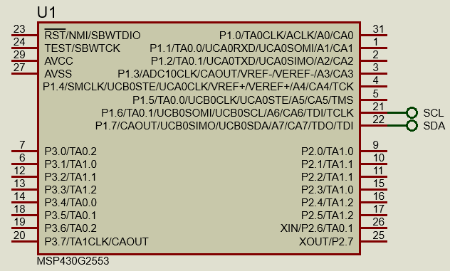
Explanation
Just like USCI SPI setup, Grace is used for setting the basic parameters for USCI I2C communication. Note only USCI_B0 supports I2C communication unlike USCI SPI communication. Since our MSP430 micro is the master device in the I2C bus, USCI module is configured as I2C master. One particular thing to observe is the I2C Slave Address. Here as shown in the screenshot below, it is 208. This is not an important figure. Same goes for the I2C Own Address part. No interrupts are to be used and so none of them are enabled.
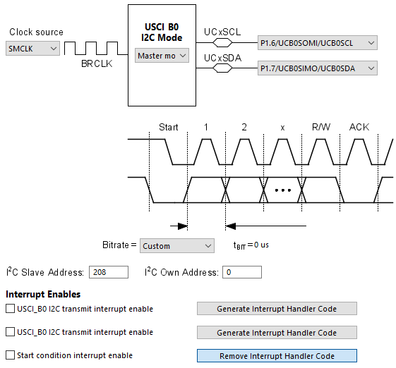
Out of the configuration set by Grace, I2C pins are set also in the I2C initialization function. This should be done manually before initializing the USCI hardware.
void I2C_USCI_init(unsigned char address)
{
P1DIR &= ~(BIT6 + BIT7);
P1OUT |= (BIT6 + BIT7);
P1SEL2 |= (BIT6 | BIT7);
P1SEL |= (BIT6 | BIT7);
UCB0CTL1 |= UCSWRST;
UCB0CTL0 = (UCMST | UCMODE_3 | UCSYNC);
UCB0CTL1 = (UCSSEL_2 | UCSWRST);
UCB0BR0 = 20;
UCB0I2CSA = address;
UCB0CTL1 &= ~UCSWRST;
}
Off all the functions used in the HW_I2C files, the following are of high importance:
unsigned char I2C_USCI_read_byte(unsigned char address);
unsigned char I2C_USCI_read_word(unsigned char address,unsigned char *value, unsigned char length);
unsigned char I2C_USCI_write_byte(unsigned char address, unsigned char value);
Their names suggest their functionality. The codes inside them are arranged as such that they take care of start-stop conditions generation, clock generation, etc. I2C communication needs device address along side read-write info. Based on read-write info, the host device writes or read I2C bus. The drawback of using I2C with these functions is the vulnerability to falling inside a loop since loops are used in these functions widely. This setback can be overcome with timeouts.
Demo
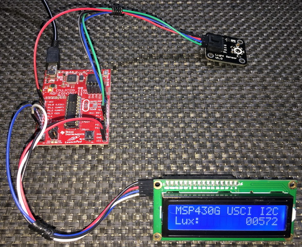
USCI I2C – Interfacing DS1307 Real Time Clock (RTC)
This part shows another example of I2C implementation using MSP430’s USCI hardware. This time the I2C device that is connected with a MSP430 is the popular DS1307 real time clock (RTC). This is the last USCI hardware example.
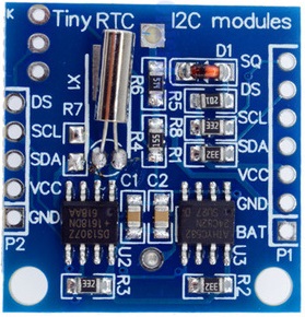
Code Example
DS1307.h
#include "HW_I2C.h"
#define DS1307_address 0x68
#define sec_reg 0x00
#define min_reg 0x01
#define hr_reg 0x02
#define day_reg 0x03
#define date_reg 0x04
#define month_reg 0x05
#define year_reg 0x06
#define control_reg 0x07
void DS1307_init(void);
unsigned char DS1307_read(unsigned char address);
void DS1307_write(unsigned char address, unsigned char value);
unsigned char bcd_to_decimal(unsigned char value);
unsigned char decimal_to_bcd(unsigned char value);
void get_time(void);
void get_date(void);
void set_time(void);
void set_date(void);
DS1307.c
#include "DS1307.h"
extern struct
{
unsigned char sec;
unsigned char min;
unsigned char hr;
unsigned char day;
unsigned char dt;
unsigned char mt;
unsigned char yr;
}rtc;
void DS1307_init(void)
{
I2C_USCI_init(DS1307_address);
DS1307_write(sec_reg, 0x00);
DS1307_write(control_reg, 0x90);
}
unsigned char DS1307_read(unsigned char address)
{
return I2C_USCI_read_byte(address);
}
void DS1307_write(unsigned char address, unsigned char value)
{
I2C_USCI_write_byte(address, value);
}
unsigned char bcd_to_decimal(unsigned char value)
{
return ((value & 0x0F) + (((value & 0xF0) >> 0x04) * 0x0A));
}
unsigned char decimal_to_bcd(unsigned char value)
{
return (((value / 0x0A) << 0x04) & 0xF0) | ((value % 0x0A) & 0x0F);
}
void get_time(void)
{
rtc.sec = DS1307_read(sec_reg);
rtc.sec = bcd_to_decimal(rtc.sec);
rtc.min = DS1307_read(min_reg);
rtc.min = bcd_to_decimal(rtc.min);
rtc.hr = DS1307_read(hr_reg);
rtc.hr = bcd_to_decimal(rtc.hr);
}
void get_date(void)
{
rtc.day = DS1307_read(day_reg);
rtc.day = bcd_to_decimal(rtc.day);
rtc.dt = DS1307_read(date_reg);
rtc.dt = bcd_to_decimal(rtc.dt);
rtc.mt = DS1307_read(month_reg);
rtc.mt = bcd_to_decimal(rtc.mt);
rtc.yr = DS1307_read(year_reg);
rtc.yr = bcd_to_decimal(rtc.yr);
}
void set_time(void)
{
rtc.sec = decimal_to_bcd(rtc.sec);
DS1307_write(sec_reg, rtc.sec);
rtc.min = decimal_to_bcd(rtc.min);
DS1307_write(min_reg, rtc.min);
rtc.hr = decimal_to_bcd(rtc.hr);
DS1307_write(hr_reg, rtc.hr);
}
void set_date(void)
{
rtc.day = decimal_to_bcd(rtc.day);
DS1307_write(day_reg, rtc.day);
rtc.dt = decimal_to_bcd(rtc.dt);
DS1307_write(date_reg, rtc.dt);
rtc.mt = decimal_to_bcd(rtc.mt);
DS1307_write(month_reg, rtc.mt);
rtc.yr = decimal_to_bcd(rtc.yr);
DS1307_write(year_reg, rtc.yr);
}
main.c
#include <msp430.h>
#include "delay.h"
#include "HW_I2C.h"
#include "DS1307.h"
#include "lcd.h"
struct
{
unsigned char sec;
unsigned char min;
unsigned char hr;
unsigned char day;
unsigned char dt;
unsigned char mt;
unsigned char yr;
}rtc;
void GPIO_graceInit(void);
void BCSplus_graceInit(void);
void USCI_B0_graceInit(void);
void System_graceInit(void);
void WDTplus_graceInit(void);
void show_value(unsigned char x_pos, unsigned char y_pos, unsigned char value);
void display_time(void);
void main(void)
{
rtc.sec = 30;
rtc.min = 58;
rtc.hr = 23;
/* Stop watchdog timer from timing out during initial start-up. */
WDTCTL = WDTPW | WDTHOLD;
/* initialize Config for the MSP430 GPIO */
GPIO_graceInit();
/* initialize Config for the MSP430 2xx family clock systems (BCS) */
BCSplus_graceInit();
/* initialize Config for the MSP430 USCI_B0 */
USCI_B0_graceInit();
/* initialize Config for the MSP430 System Registers */
System_graceInit();
/* initialize Config for the MSP430 WDT+ */
WDTplus_graceInit();
LCD_init();
LCD_clear_home();
LCD_goto(0, 0);
LCD_putstr("MSP430G USCI I2C");
DS1307_init();
set_time();
while(1)
{
get_time();
display_time();
}
}
void GPIO_graceInit(void)
{
/* USER CODE START (section: GPIO_graceInit_prologue) */
/* User initialization code */
/* USER CODE END (section: GPIO_graceInit_prologue) */
/* Port 1 Port Select 2 Register */
P1SEL2 = BIT6 | BIT7;
/* Port 1 Output Register */
P1OUT = 0;
/* Port 1 Port Select Register */
P1SEL = BIT6 | BIT7;
/* Port 1 Direction Register */
P1DIR = 0;
/* Port 1 Interrupt Edge Select Register */
P1IES = 0;
/* Port 1 Interrupt Flag Register */
P1IFG = 0;
/* Port 2 Output Register */
P2OUT = 0;
/* Port 2 Direction Register */
P2DIR = 0;
/* Port 2 Interrupt Edge Select Register */
P2IES = 0;
/* Port 2 Interrupt Flag Register */
P2IFG = 0;
/* Port 3 Output Register */
P3OUT = 0;
/* Port 3 Direction Register */
P3DIR = 0;
/* USER CODE START (section: GPIO_graceInit_epilogue) */
/* User code */
/* USER CODE END (section: GPIO_graceInit_epilogue) */
}
void BCSplus_graceInit(void)
{
/* USER CODE START (section: BCSplus_graceInit_prologue) */
/* User initialization code */
/* USER CODE END (section: BCSplus_graceInit_prologue) */
/*
* Basic Clock System Control 2
*
* SELM_0 -- DCOCLK
* DIVM_0 -- Divide by 1
* ~SELS -- DCOCLK
* DIVS_0 -- Divide by 1
* ~DCOR -- DCO uses internal resistor
*
* Note: ~<BIT> indicates that <BIT> has value zero
*/
BCSCTL2 = SELM_0 | DIVM_0 | DIVS_0;
if (CALBC1_1MHZ != 0xFF)
{
/* Follow recommended flow. First, clear all DCOx and MODx bits. Then
* apply new RSELx values. Finally, apply new DCOx and MODx bit values.
*/
DCOCTL = 0x00;
BCSCTL1 = CALBC1_1MHZ; /* Set DCO to 1MHz */
DCOCTL = CALDCO_1MHZ;
}
/*
* Basic Clock System Control 1
*
* XT2OFF -- Disable XT2CLK
* ~XTS -- Low Frequency
* DIVA_0 -- Divide by 1
*
* Note: ~XTS indicates that XTS has value zero
*/
BCSCTL1 |= XT2OFF | DIVA_0;
/*
* Basic Clock System Control 3
*
* XT2S_0 -- 0.4 - 1 MHz
* LFXT1S_0 -- If XTS = 0, XT1 = 32768kHz Crystal ; If XTS = 1, XT1 = 0.4 - 1-MHz crystal or resonator
* XCAP_1 -- ~6 pF
*/
BCSCTL3 = XT2S_0 | LFXT1S_0 | XCAP_1;
/* USER CODE START (section: BCSplus_graceInit_epilogue) */
/* User code */
/* USER CODE END (section: BCSplus_graceInit_epilogue) */
}
void USCI_B0_graceInit(void)
{
/* USER CODE START (section: USCI_B0_graceInit_prologue) */
/* User initialization code */
/* USER CODE END (section: USCI_B0_graceInit_prologue) */
/* Disable USCI */
UCB0CTL1 |= UCSWRST;
/*
* Control Register 0
*
* ~UCA10 -- Own address is a 7-bit address
* ~UCSLA10 -- Address slave with 7-bit address
* ~UCMM -- Single master environment. There is no other master in the system. The address compare unit is disabled
* UCMST -- Master mode
* UCMODE_3 -- I2C Mode
* UCSYNC -- Synchronous Mode
*
* Note: ~<BIT> indicates that <BIT> has value zero
*/
UCB0CTL0 = UCMST | UCMODE_3 | UCSYNC;
/*
* Control Register 1
*
* UCSSEL_2 -- SMCLK
* ~UCTR -- Receiver
* ~UCTXNACK -- Acknowledge normally
* ~UCTXSTP -- No STOP generated
* ~UCTXSTT -- Do not generate START condition
* UCSWRST -- Enabled. USCI logic held in reset state
*
* Note: ~<BIT> indicates that <BIT> has value zero
*/
UCB0CTL1 = UCSSEL_2 | UCSWRST;
/* I2C Slave Address Register */
UCB0I2CSA = DS1307_address;
/* Bit Rate Control Register 0 */
UCB0BR0 = 20;
/* Enable USCI */
UCB0CTL1 &= ~UCSWRST;
/* USER CODE START (section: USCI_B0_graceInit_epilogue) */
/* User code */
/* USER CODE END (section: USCI_B0_graceInit_epilogue) */
}
void System_graceInit(void)
{
/* USER CODE START (section: System_graceInit_prologue) */
/* User initialization code */
/* USER CODE END (section: System_graceInit_prologue) */
/*
* SR, Status Register
*
* ~SCG1 -- Disable System clock generator 1
* ~SCG0 -- Disable System clock generator 0
* ~OSCOFF -- Oscillator On
* ~CPUOFF -- CPU On
* GIE -- General interrupt enable
*
* Note: ~<BIT> indicates that <BIT> has value zero
*/
__bis_SR_register(GIE);
/* USER CODE START (section: System_graceInit_epilogue) */
/* User code */
/* USER CODE END (section: System_graceInit_epilogue) */
}
void WDTplus_graceInit(void)
{
/* USER CODE START (section: RTC_B_graceInit_prologue) */
/* User initialization code */
/* USER CODE END (section: RTC_B_graceInit_prologue) */
/*
* WDTCTL, Watchdog Timer+ Register
*
* WDTPW -- Watchdog password
* WDTHOLD -- Watchdog timer+ is stopped
* ~WDTNMIES -- NMI on rising edge
* ~WDTNMI -- Reset function
* ~WDTTMSEL -- Watchdog mode
* ~WDTCNTCL -- No action
* ~WDTSSEL -- SMCLK
* ~WDTIS0 -- Watchdog clock source bit0 disabled
* ~WDTIS1 -- Watchdog clock source bit1 disabled
*
* Note: ~<BIT> indicates that <BIT> has value zero
*/
WDTCTL = WDTPW | WDTHOLD;
/* USER CODE START (section: RTC_B_graceInit_epilogue) */
/* User code */
/* USER CODE END (section: RTC_B_graceInit_epilogue) */
}
void show_value(unsigned char x_pos, unsigned char y_pos, unsigned char value)
{
char chr = 0;
chr = ((value / 10) + 0x30);
LCD_goto(x_pos, y_pos);
LCD_putchar(chr);
chr = ((value % 10) + 0x30);
LCD_goto((x_pos + 1), y_pos);
LCD_putchar(chr);
}
void display_time(void)
{
LCD_goto(6, 1);
LCD_putchar(' ');
LCD_goto(9, 1);
LCD_putchar(' ');
delay_ms(450);
show_value(7, 1, rtc.hr);
show_value(10, 1, rtc.min);
show_value(4, 1, rtc.sec);
LCD_goto(6, 1);
LCD_putchar(':');
LCD_goto(9, 1);
LCD_putchar(':');
delay_ms(450);
}
Simulation
DS1307 simulation encountered some weird issues but it does work.
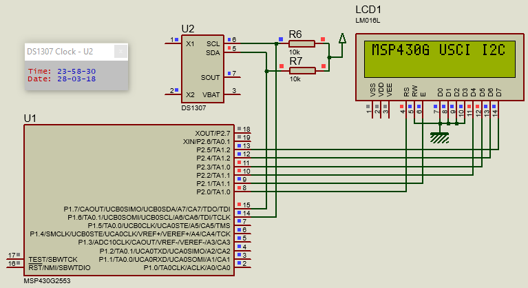
Explanation
Since it uses the same ideas as in the previous example, there is hardly a thing to explain here.
Demo
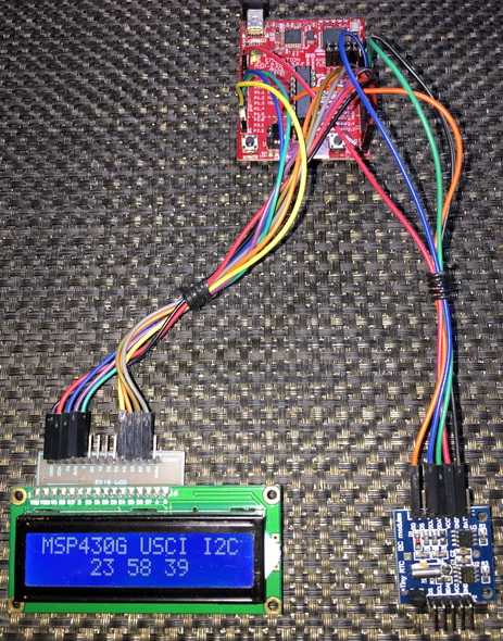
ADC10 with Direct Memory Access (DMA)
The concept of Direct Memory Access (DMA) or Data Transfer Controller (DTC) is usually found in 32-bit ARM-Cortex-based micros and in some highly advanced DSP microcontrollers. In recent times, a few new generation 8-bit and 16-bit devices have emerged with DMA hardware feature. The DMA hardware may look a bit complicated for those who are new to it but it is practically very simple. Just consider what you have been doing all these times without DMA. Consider an ADC for an example. Without DMA, the ADC senses its channel(s) and saves sensed data on an ADC result register waiting to be read and continue the same operation over and over again. This process involves the CPU very often as sensing/extracting analog data, storing it and starting ADC conversion all needs CPU’s attention. Thus, the CPU bus is always busy with these engagements. With DMA the process becomes more automatic and intelligent. The DMA controller automatically transfers AD conversion data to specified memory location(s) using its separate data bus. In the whole process the CPU is not involved much. Conversions take place and the conversion results are immediately transferred. Thus, the process becomes both autonomous and fast.
Please note that the DMA bus is only available for ADC to memory or in other words peripheral to memory transfers. It cannot be used for other peripherals like USCI, USI, etc. or for memory-memory transfers. However, it is not a big issue for now.
Code Example
#include <msp430.h>
#include "delay.h"
#include "SW_I2C.h"
#include "PCF8574.h"
#include "lcd.h"
#define no_of_samples 16
unsigned int adc_pointer[no_of_samples];
void GPIO_graceInit(void);
void BCSplus_graceInit(void);
void ADC10_graceInit(void);
void System_graceInit(void);
void WDTplus_graceInit(void);
void lcd_print(unsigned char x_pos, unsigned char y_pos, unsigned int value);
void main(void)
{
unsigned char s = 0;
unsigned int adc_avg = 0;
/* Stop watchdog timer from timing out during initial start-up. */
WDTCTL = WDTPW | WDTHOLD;
/* initialize Config for the MSP430 GPIO */
GPIO_graceInit();
/* initialize Config for the MSP430 2xx family clock systems (BCS) */
BCSplus_graceInit();
/* initialize Config for the MSP430 10-bit Analog to Digital Converter (ADC) */
ADC10_graceInit();
/* initialize Config for the MSP430 System Registers */
System_graceInit();
/* initialize Config for the MSP430 WDT+ */
WDTplus_graceInit();
LCD_init();
LCD_clear_home();
LCD_goto(0, 0);
LCD_putstr("MSP430 ADC + DMA:");
LCD_goto(0, 1);
LCD_putstr("A1:");
while(1)
{
adc_avg = 0;
P1OUT |= BIT0;
ADC10CTL0 &= ~ENC;
while (ADC10CTL1 & BUSY);
ADC10CTL0 |= (ENC | ADC10SC);
for(s = 0; s < no_of_samples; s++)
{
adc_avg += adc_pointer[s];
}
adc_avg = (adc_avg / no_of_samples);
lcd_print(12, 1, adc_avg);
delay_ms(100);
P1OUT &= ~BIT0;
delay_ms(100);
};
}
void GPIO_graceInit(void)
{
/* USER CODE START (section: GPIO_graceInit_prologue) */
/* User initialization code */
/* USER CODE END (section: GPIO_graceInit_prologue) */
/* Port 1 Output Register */
P1OUT = 0;
/* Port 1 Direction Register */
P1DIR = BIT0;
/* Port 1 Interrupt Edge Select Register */
P1IES = 0;
/* Port 1 Interrupt Flag Register */
P1IFG = 0;
/* Port 2 Output Register */
P2OUT = 0;
/* Port 2 Direction Register */
P2DIR = 0;
/* Port 2 Interrupt Edge Select Register */
P2IES = 0;
/* Port 2 Interrupt Flag Register */
P2IFG = 0;
/* USER CODE START (section: GPIO_graceInit_epilogue) */
/* User code */
/* USER CODE END (section: GPIO_graceInit_epilogue) */
}
void BCSplus_graceInit(void)
{
/* USER CODE START (section: BCSplus_graceInit_prologue) */
/* User initialization code */
/* USER CODE END (section: BCSplus_graceInit_prologue) */
/*
* Basic Clock System Control 2
*
* SELM_0 -- DCOCLK
* DIVM_0 -- Divide by 1
* ~SELS -- DCOCLK
* DIVS_0 -- Divide by 1
* ~DCOR -- DCO uses internal resistor
*
* Note: ~<BIT> indicates that <BIT> has value zero
*/
BCSCTL2 = SELM_0 | DIVM_0 | DIVS_0;
if (CALBC1_8MHZ != 0xFF)
{
/* Adjust this accordingly to your VCC rise time */
__delay_cycles(100000);
// Follow recommended flow. First, clear all DCOx and MODx bits. Then
// apply new RSELx values. Finally, apply new DCOx and MODx bit values.
DCOCTL = 0x00;
BCSCTL1 = CALBC1_8MHZ; /* Set DCO to 8MHz */
DCOCTL = CALDCO_8MHZ;
}
/*
* Basic Clock System Control 1
*
* XT2OFF -- Disable XT2CLK
* ~XTS -- Low Frequency
* DIVA_0 -- Divide by 1
*
* Note: ~XTS indicates that XTS has value zero
*/
BCSCTL1 |= XT2OFF | DIVA_0;
/*
* Basic Clock System Control 3
*
* XT2S_0 -- 0.4 - 1 MHz
* LFXT1S_2 -- If XTS = 0, XT1 = VLOCLK ; If XTS = 1, XT1 = 3 - 16-MHz crystal or resonator
* XCAP_1 -- ~6 pF
*/
BCSCTL3 = XT2S_0 | LFXT1S_2 | XCAP_1;
/* USER CODE START (section: BCSplus_graceInit_epilogue) */
/* User code */
/* USER CODE END (section: BCSplus_graceInit_epilogue) */
}
void ADC10_graceInit(void)
{
/* USER CODE START (section: ADC10_graceInit_prologue) */
/* User initialization code */
/* USER CODE END (section: ADC10_graceInit_prologue) */
/* disable ADC10 during initialization */
ADC10CTL0 &= ~ENC;
/*
* Control Register 0
*
* ~ADC10SC -- No conversion
* ~ENC -- Disable ADC
* ~ADC10IFG -- Clear ADC interrupt flag
* ~ADC10IE -- Disable ADC interrupt
* ADC10ON -- Switch On ADC10
* ~REFON -- Disable ADC reference generator
* ~REF2_5V -- Set reference voltage generator = 1.5V
* MSC -- Enable multiple sample and conversion
* ~REFBURST -- Reference buffer on continuously
* ~REFOUT -- Reference output off
* ~ADC10SR -- Reference buffer supports up to ~200 ksps
* ADC10SHT_2 -- 16 x ADC10CLKs
* SREF_0 -- VR+ = VCC and VR- = VSS
*
* Note: ~<BIT> indicates that <BIT> has value zero
*/
ADC10CTL0 = ADC10ON | MSC | ADC10SHT_2 | SREF_0;
/*
* Control Register 1
*
* ~ADC10BUSY -- No operation is active
* CONSEQ_2 -- Repeat single channel
* ADC10SSEL_0 -- ADC10OSC
* ADC10DIV_0 -- Divide by 1
* ~ISSH -- Input signal not inverted
* ~ADC10DF -- ADC10 Data Format as binary
* SHS_0 -- ADC10SC
* INCH_1 -- ADC Channel 1
*
* Note: ~<BIT> indicates that <BIT> has value zero
*/
ADC10CTL1 = CONSEQ_2 | ADC10SSEL_0 | ADC10DIV_0 | SHS_0 | INCH_1;
/* Analog (Input) Enable Control Register 0 */
ADC10AE0 = 0x2;
/*
* Data Transfer Control Register 0
*
* ~ADC10TB -- One-block transfer mode
* ADC10CT -- Data is transferred continuously after every conversion
*
* Note: ~ADC10TB indicates that ADC10TB has value zero
*/
ADC10DTC0 = ADC10CT;
/* Data Transfer Control Register 1 */
ADC10DTC1 = no_of_samples;
/* Data Transfer Start Address */
ADC10SA = ((unsigned int)adc_pointer);
/* enable ADC10 */
ADC10CTL0 |= ENC;
/* USER CODE START (section: ADC10_graceInit_epilogue) */
/* User code */
/* USER CODE END (section: ADC10_graceInit_epilogue) */
}
void System_graceInit(void)
{
/* USER CODE START (section: System_graceInit_prologue) */
/* User initialization code */
/* USER CODE END (section: System_graceInit_prologue) */
/* Clear oscillator fault flag with software delay */
do
{
// Clear OSC fault flag
IFG1 &= ~OFIFG;
// 50us delay
__delay_cycles(400);
} while (IFG1 & OFIFG);
/*
* SR, Status Register
*
* ~SCG1 -- Disable System clock generator 1
* ~SCG0 -- Disable System clock generator 0
* ~OSCOFF -- Oscillator On
* ~CPUOFF -- CPU On
* GIE -- General interrupt enable
*
* Note: ~<BIT> indicates that <BIT> has value zero
*/
__bis_SR_register(GIE);
/* USER CODE START (section: System_graceInit_epilogue) */
/* User code */
/* USER CODE END (section: System_graceInit_epilogue) */
}
void WDTplus_graceInit(void)
{
/* USER CODE START (section: RTC_B_graceInit_prologue) */
/* User initialization code */
/* USER CODE END (section: RTC_B_graceInit_prologue) */
/*
* WDTCTL, Watchdog Timer+ Register
*
* WDTPW -- Watchdog password
* WDTHOLD -- Watchdog timer+ is stopped
* ~WDTNMIES -- NMI on rising edge
* ~WDTNMI -- Reset function
* ~WDTTMSEL -- Watchdog mode
* ~WDTCNTCL -- No action
* ~WDTSSEL -- SMCLK
* ~WDTIS0 -- Watchdog clock source bit0 disabled
* ~WDTIS1 -- Watchdog clock source bit1 disabled
*
* Note: ~<BIT> indicates that <BIT> has value zero
*/
WDTCTL = WDTPW | WDTHOLD;
/* USER CODE START (section: RTC_B_graceInit_epilogue) */
/* User code */
/* USER CODE END (section: RTC_B_graceInit_epilogue) */
}
void lcd_print(unsigned char x_pos, unsigned char y_pos, unsigned int value)
{
char chr = 0;
chr = ((value / 1000) + 0x30);
LCD_goto(x_pos, y_pos);
LCD_putchar(chr);
chr = (((value / 100) % 10) + 0x30);
LCD_goto((x_pos + 1), y_pos);
LCD_putchar(chr);
chr = (((value / 10) % 10) + 0x30);
LCD_goto((x_pos + 2), y_pos);
LCD_putchar(chr);
chr = ((value % 10) + 0x30);
LCD_goto((x_pos + 3), y_pos);
LCD_putchar(chr);
}
Simulation
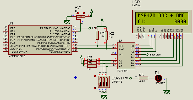
Explanation
Use Power User setup screen of Grace to configure the DTC. Observe the setup as shown below:
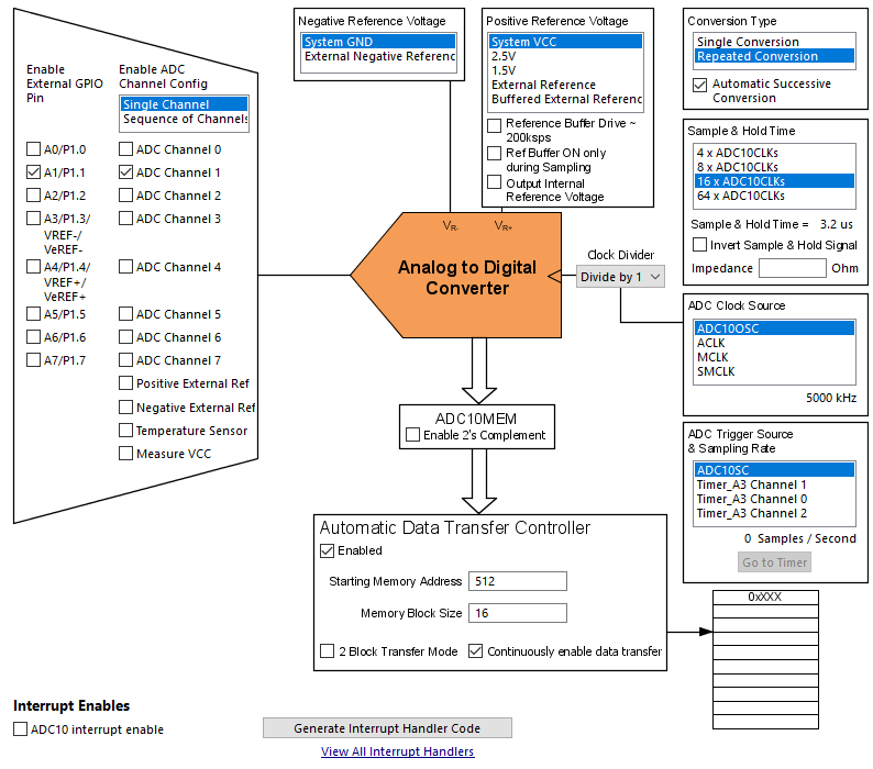
Here only channel 1 was used. The setup is similar to the first ADC10 example setup. The main difference is the enabling of the DTC block. Note the starting memory address and the memory block size. The memory we are talking about here is no other than MSP430’s RAM. Unless you want to assign a different pointer address, keep it untouched. So why is it pointed at RAM location 512 (0x200) by default? The answer is the fact that this is first RAM location for our target MSP430G2452 microcontroller. Check the memory map below:
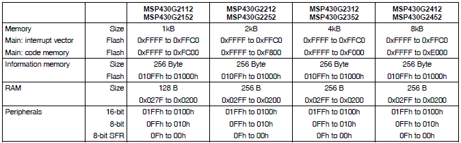
The block size indicates that number of locations that we will need to store ADC10 data. MSP430s are 16-bit microcontrollers and since ADC10 gives 10-bit data, we need sixteen word-sized (16-bit) locations to store sixteen ADC samples. These 16 samples are to be averaged.
#define no_of_samples 16
....
unsigned int adc_pointer[no_of_samples];
....
....
ADC10DTC1 = no_of_samples;
ADC10SA = ((unsigned int)adc_pointer);
Grace generates the initialization code but the above lines must be edited by the coder.
In the main function, ADC10 is commanded to begin and store conversions. Once all sixteen ADC10 data are captured, they are summed up and averaged. The averaged data is shown on a LCD screen. Note that ADC10 interrupt is not used and not anywhere in the code the ADC10MEM register is directly read. The ADC is read and processed by the DMA, freeing up the CPU for other tasks. The process is repetitive, automomous and continuous.
adc_avg = 0;
P1OUT |= BIT0;
ADC10CTL0 &= ~ENC;
while (ADC10CTL1 & BUSY);
ADC10CTL0 |= (ENC | ADC10SC);
for(s = 0; s < no_of_samples; s++)
{
adc_avg += adc_pointer[s];
}
adc_avg = (adc_avg / no_of_samples);
lcd_print(12, 1, adc_avg);
delay_ms(100);
P1OUT &= ~BIT0;
delay_ms(100);
Demo
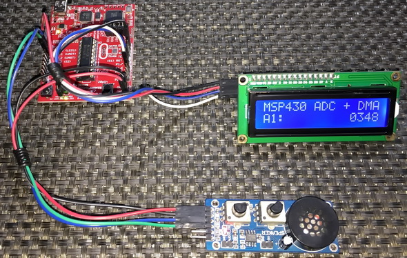
Sensing a Sequence of ADC10 Channels with DMA
We have seen in the last segment that how we can compute the average value of an ADC10 channel without involving the CPU much and using the MSP430’s DMA/DTC controller. The DTC of MSP430s can be used in many innovative ways. One such way is to sense multiple channels in a row. In this method, the ADC is basically scanned in an orderly fashion from the coder-specified topmost channel to the bottommost (channel 0), saving the result of each ADC channel conversion in separate memory locations. Scanning a sequence of AD channels in this way has many potential applications. Consider the case of a solar charger controller. With one command you get both the input and output voltages, and currents quickly from your MSP430 micro. DMA-assisted ADC scanning is perhaps the most efficient and simple way to sense multiple ADC channels quickly.
Code Example
#include <msp430.h>
#include "delay.h"
#include "SW_I2C.h"
#include "PCF8574.h"
#include "lcd.h"
unsigned int ADC_value[2] = {0, 0};
void GPIO_graceInit(void);
void BCSplus_graceInit(void);
void ADC10_graceInit(void);
void System_graceInit(void);
void WDTplus_graceInit(void);
void lcd_print(unsigned char x_pos, unsigned char y_pos, unsigned int value);
void main(void)
{
/* Stop watchdog timer from timing out during initial start-up. */
WDTCTL = WDTPW | WDTHOLD;
/* initialize Config for the MSP430 GPIO */
GPIO_graceInit();
/* initialize Config for the MSP430 2xx family clock systems (BCS) */
BCSplus_graceInit();
/* initialize Config for the MSP430 10-bit Analog to Digital Converter (ADC) */
ADC10_graceInit();
/* initialize Config for the MSP430 System Registers */
System_graceInit();
/* initialize Config for the MSP430 WDT+ */
WDTplus_graceInit();
LCD_init();
LCD_clear_home();
LCD_goto(0, 0);
LCD_putstr("A0:");
LCD_goto(0, 1);
LCD_putstr("A1:");
while(1)
{
ADC10CTL0 &= ~ENC;
while (ADC10CTL1 & BUSY);
ADC10CTL0 |= (ENC | ADC10SC);
lcd_print(12, 0, ADC_value[1]);
lcd_print(12, 1, ADC_value[0]);
delay_ms(400);
};
}
void GPIO_graceInit(void)
{
/* USER CODE START (section: GPIO_graceInit_prologue) */
/* User initialization code */
/* USER CODE END (section: GPIO_graceInit_prologue) */
/* Port 1 Output Register */
P1OUT = 0;
/* Port 1 Direction Register */
P1DIR = 0;
/* Port 1 Interrupt Edge Select Register */
P1IES = 0;
/* Port 1 Interrupt Flag Register */
P1IFG = 0;
/* Port 2 Output Register */
P2OUT = 0;
/* Port 2 Direction Register */
P2DIR = 0;
/* Port 2 Interrupt Edge Select Register */
P2IES = 0;
/* Port 2 Interrupt Flag Register */
P2IFG = 0;
/* USER CODE START (section: GPIO_graceInit_epilogue) */
/* User code */
/* USER CODE END (section: GPIO_graceInit_epilogue) */
}
void BCSplus_graceInit(void)
{
/* USER CODE START (section: BCSplus_graceInit_prologue) */
/* User initialization code */
/* USER CODE END (section: BCSplus_graceInit_prologue) */
/*
* Basic Clock System Control 2
*
* SELM_0 -- DCOCLK
* DIVM_0 -- Divide by 1
* ~SELS -- DCOCLK
* DIVS_0 -- Divide by 1
* ~DCOR -- DCO uses internal resistor
*
* Note: ~<BIT> indicates that <BIT> has value zero
*/
BCSCTL2 = SELM_0 | DIVM_0 | DIVS_0;
if (CALBC1_8MHZ != 0xFF)
{
/* Adjust this accordingly to your VCC rise time */
__delay_cycles(100000);
// Follow recommended flow. First, clear all DCOx and MODx bits. Then
// apply new RSELx values. Finally, apply new DCOx and MODx bit values.
DCOCTL = 0x00;
BCSCTL1 = CALBC1_8MHZ; /* Set DCO to 8MHz */
DCOCTL = CALDCO_8MHZ;
}
/*
* Basic Clock System Control 1
*
* XT2OFF -- Disable XT2CLK
* ~XTS -- Low Frequency
* DIVA_0 -- Divide by 1
*
* Note: ~XTS indicates that XTS has value zero
*/
BCSCTL1 |= XT2OFF | DIVA_0;
/*
* Basic Clock System Control 3
*
* XT2S_0 -- 0.4 - 1 MHz
* LFXT1S_2 -- If XTS = 0, XT1 = VLOCLK ; If XTS = 1, XT1 = 3 - 16-MHz crystal or resonator
* XCAP_1 -- ~6 pF
*/
BCSCTL3 = XT2S_0 | LFXT1S_2 | XCAP_1;
/* USER CODE START (section: BCSplus_graceInit_epilogue) */
/* User code */
/* USER CODE END (section: BCSplus_graceInit_epilogue) */
}
void ADC10_graceInit(void)
{
/* USER CODE START (section: ADC10_graceInit_prologue) */
/* User initialization code */
/* USER CODE END (section: ADC10_graceInit_prologue) */
/* disable ADC10 during initialization */
ADC10CTL0 &= ~ENC;
/*
* Control Register 0
*
* ~ADC10SC -- No conversion
* ~ENC -- Disable ADC
* ~ADC10IFG -- Clear ADC interrupt flag
* ~ADC10IE -- Disable ADC interrupt
* ADC10ON -- Switch On ADC10
* ~REFON -- Disable ADC reference generator
* ~REF2_5V -- Set reference voltage generator = 1.5V
* MSC -- Enable multiple sample and conversion
* ~REFBURST -- Reference buffer on continuously
* ~REFOUT -- Reference output off
* ~ADC10SR -- Reference buffer supports up to ~200 ksps
* ADC10SHT_2 -- 16 x ADC10CLKs
* SREF_0 -- VR+ = VCC and VR- = VSS
*
* Note: ~<BIT> indicates that <BIT> has value zero
*/
ADC10CTL0 = ADC10ON | MSC | ADC10SHT_2 | SREF_0;
/*
* Control Register 1
*
* ~ADC10BUSY -- No operation is active
* CONSEQ_3 -- Repeat sequence of channels
* ADC10SSEL_0 -- ADC10OSC
* ADC10DIV_0 -- Divide by 1
* ~ISSH -- Input signal not inverted
* ~ADC10DF -- ADC10 Data Format as binary
* SHS_0 -- ADC10SC
* INCH_1 -- ADC Channel 1
*
* Note: ~<BIT> indicates that <BIT> has value zero
*/
ADC10CTL1 = CONSEQ_3 | ADC10SSEL_0 | ADC10DIV_0 | SHS_0 | INCH_1;
/* Analog (Input) Enable Control Register 0 */
ADC10AE0 = 0x3;
/*
* Data Transfer Control Register 0
*
* ~ADC10TB -- One-block transfer mode
* ADC10CT -- Data is transferred continuously after every conversion
*
* Note: ~ADC10TB indicates that ADC10TB has value zero
*/
ADC10DTC0 = ADC10CT;
/* Data Transfer Control Register 1 */
ADC10DTC1 = 2;
/* Data Transfer Start Address */
ADC10SA = ((unsigned int)ADC_value);
/* enable ADC10 */
ADC10CTL0 |= ENC;
/* USER CODE START (section: ADC10_graceInit_epilogue) */
/* User code */
/* USER CODE END (section: ADC10_graceInit_epilogue) */
}
void System_graceInit(void)
{
/* USER CODE START (section: System_graceInit_prologue) */
/* User initialization code */
/* USER CODE END (section: System_graceInit_prologue) */
/* Clear oscillator fault flag with software delay */
do
{
// Clear OSC fault flag
IFG1 &= ~OFIFG;
// 50us delay
__delay_cycles(400);
} while (IFG1 & OFIFG);
/*
* SR, Status Register
*
* ~SCG1 -- Disable System clock generator 1
* ~SCG0 -- Disable System clock generator 0
* ~OSCOFF -- Oscillator On
* ~CPUOFF -- CPU On
* GIE -- General interrupt enable
*
* Note: ~<BIT> indicates that <BIT> has value zero
*/
__bis_SR_register(GIE);
/* USER CODE START (section: System_graceInit_epilogue) */
/* User code */
/* USER CODE END (section: System_graceInit_epilogue) */
}
void WDTplus_graceInit(void)
{
/* USER CODE START (section: RTC_B_graceInit_prologue) */
/* User initialization code */
/* USER CODE END (section: RTC_B_graceInit_prologue) */
/*
* WDTCTL, Watchdog Timer+ Register
*
* WDTPW -- Watchdog password
* WDTHOLD -- Watchdog timer+ is stopped
* ~WDTNMIES -- NMI on rising edge
* ~WDTNMI -- Reset function
* ~WDTTMSEL -- Watchdog mode
* ~WDTCNTCL -- No action
* ~WDTSSEL -- SMCLK
* ~WDTIS0 -- Watchdog clock source bit0 disabled
* ~WDTIS1 -- Watchdog clock source bit1 disabled
*
* Note: ~<BIT> indicates that <BIT> has value zero
*/
WDTCTL = WDTPW | WDTHOLD;
/* USER CODE START (section: RTC_B_graceInit_epilogue) */
/* User code */
/* USER CODE END (section: RTC_B_graceInit_epilogue) */
}
void lcd_print(unsigned char x_pos, unsigned char y_pos, unsigned int value)
{
char chr = 0;
chr = ((value / 1000) + 0x30);
LCD_goto(x_pos, y_pos);
LCD_putchar(chr);
chr = (((value / 100) % 10) + 0x30);
LCD_goto((x_pos + 1), y_pos);
LCD_putchar(chr);
chr = (((value / 10) % 10) + 0x30);
LCD_goto((x_pos + 2), y_pos);
LCD_putchar(chr);
chr = ((value % 10) + 0x30);
LCD_goto((x_pos + 3), y_pos);
LCD_putchar(chr);
}
Simulation
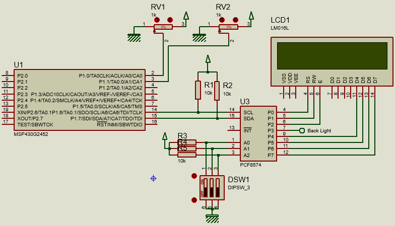
Explanation
Except some minor differences, the Grace setup here is same as the one used in the DMA example. The first difference is the Sequence of Channels selection, second is the number of ADC channels and finally the size of memory block.
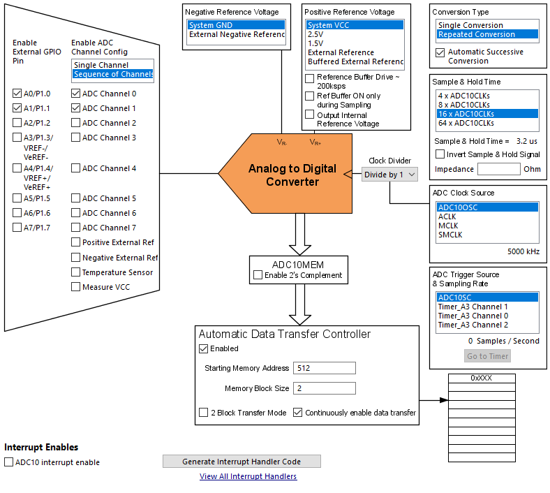
In the main, most of the things are same as in the DMA example. Since two channels are read, two memory locations store individual ADC data. Scanning starts from topmost channel to the bottommost and so the bottommost memory location will hold the data of the topmost channel and vice versa. In short, the memory locations are flipped with respect to ADC channels.
ADC10CTL0 &= ~ENC;
while (ADC10CTL1 & BUSY);
ADC10CTL0 |= (ENC | ADC10SC);
lcd_print(12, 0, ADC_value[1]);
lcd_print(12, 1, ADC_value[0]);
delay_ms(400);
Demo
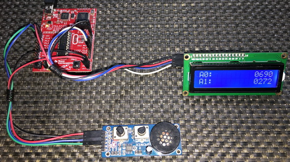
Sensing Multiple Out-of-Sequence ADC10 Channels with DMA
Due to several obligations and design constraints, we may often fall in situations where we would not be able to enjoy the sequential DTC-assisted ADC scanning feature demonstrated in the previous section. ADC channels may not be in an orderly sequence. Still we can apply similar techniques as in ADC scanning but certain things are needed to be kept in mind in such cases.
Code Example
#include <msp430.h>
#include "delay.h"
#include "SW_I2C.h"
#include "PCF8574.h"
#include "lcd.h"
#define no_of_channels 12
unsigned int ADC_value[no_of_channels];
void GPIO_graceInit(void);
void BCSplus_graceInit(void);
void ADC10_graceInit(void);
void System_graceInit(void);
void WDTplus_graceInit(void);
void lcd_print(unsigned char x_pos, unsigned char y_pos, unsigned int value);
void main(void)
{
/* Stop watchdog timer from timing out during initial start-up. */
WDTCTL = WDTPW | WDTHOLD;
/* initialize Config for the MSP430 GPIO */
GPIO_graceInit();
/* initialize Config for the MSP430 2xx family clock systems (BCS) */
BCSplus_graceInit();
/* initialize Config for the MSP430 10-bit Analog to Digital Converter (ADC) */
ADC10_graceInit();
/* initialize Config for the MSP430 System Registers */
System_graceInit();
/* initialize Config for the MSP430 WDT+ */
WDTplus_graceInit();
LCD_init();
LCD_clear_home();
while(1)
{
ADC10CTL0 &= ~ENC;
while (ADC10CTL1 & BUSY);
ADC10CTL0 |= (ENC | ADC10SC);
LCD_goto(0, 0);
LCD_putstr("A03:");
lcd_print(12, 0, ADC_value[8]);
LCD_goto(0, 1);
LCD_putstr("A11:");
lcd_print(12, 1, ADC_value[0]);
P1OUT ^= BIT0;
delay_ms(900);
ADC10CTL0 &= ~ENC;
while (ADC10CTL1 & BUSY);
ADC10CTL0 |= (ENC | ADC10SC);
LCD_goto(0, 0);
LCD_putstr("A00:");
lcd_print(12, 0, ADC_value[11]);
LCD_goto(0, 1);
LCD_putstr("A10:");
lcd_print(12, 1, ADC_value[1]);
P1OUT ^= BIT0;
delay_ms(900);
};
}
void GPIO_graceInit(void)
{
/* USER CODE START (section: GPIO_graceInit_prologue) */
/* User initialization code */
/* USER CODE END (section: GPIO_graceInit_prologue) */
/* Port 1 Output Register */
P1OUT = 0;
/* Port 1 Direction Register */
P1DIR = BIT0;
/* Port 1 Interrupt Edge Select Register */
P1IES = 0;
/* Port 1 Interrupt Flag Register */
P1IFG = 0;
/* Port 2 Output Register */
P2OUT = 0;
/* Port 2 Port Select Register */
P2SEL &= ~(BIT6 | BIT7);
/* Port 2 Direction Register */
P2DIR = 0;
/* Port 2 Interrupt Edge Select Register */
P2IES = 0;
/* Port 2 Interrupt Flag Register */
P2IFG = 0;
/* USER CODE START (section: GPIO_graceInit_epilogue) */
/* User code */
/* USER CODE END (section: GPIO_graceInit_epilogue) */
}
void BCSplus_graceInit(void)
{
/* USER CODE START (section: BCSplus_graceInit_prologue) */
/* User initialization code */
/* USER CODE END (section: BCSplus_graceInit_prologue) */
/*
* Basic Clock System Control 2
*
* SELM_0 -- DCOCLK
* DIVM_0 -- Divide by 1
* ~SELS -- DCOCLK
* DIVS_0 -- Divide by 1
* ~DCOR -- DCO uses internal resistor
*
* Note: ~<BIT> indicates that <BIT> has value zero
*/
BCSCTL2 = SELM_0 | DIVM_0 | DIVS_0;
if (CALBC1_8MHZ != 0xFF)
{
/* Adjust this accordingly to your VCC rise time */
__delay_cycles(100000);
// Follow recommended flow. First, clear all DCOx and MODx bits. Then
// apply new RSELx values. Finally, apply new DCOx and MODx bit values.
DCOCTL = 0x00;
BCSCTL1 = CALBC1_8MHZ; /* Set DCO to 8MHz */
DCOCTL = CALDCO_8MHZ;
}
/*
* Basic Clock System Control 1
*
* XT2OFF -- Disable XT2CLK
* ~XTS -- Low Frequency
* DIVA_0 -- Divide by 1
*
* Note: ~XTS indicates that XTS has value zero
*/
BCSCTL1 |= XT2OFF | DIVA_0;
/*
* Basic Clock System Control 3
*
* XT2S_0 -- 0.4 - 1 MHz
* LFXT1S_2 -- If XTS = 0, XT1 = VLOCLK ; If XTS = 1, XT1 = 3 - 16-MHz crystal or resonator
* XCAP_1 -- ~6 pF
*/
BCSCTL3 = XT2S_0 | LFXT1S_2 | XCAP_1;
/* USER CODE START (section: BCSplus_graceInit_epilogue) */
/* User code */
/* USER CODE END (section: BCSplus_graceInit_epilogue) */
}
void ADC10_graceInit(void)
{
/* USER CODE START (section: ADC10_graceInit_prologue) */
/* User initialization code */
/* USER CODE END (section: ADC10_graceInit_prologue) */
/* disable ADC10 during initialization */
ADC10CTL0 &= ~ENC;
/*
* Control Register 0
*
* ~ADC10SC -- No conversion
* ~ENC -- Disable ADC
* ~ADC10IFG -- Clear ADC interrupt flag
* ~ADC10IE -- Disable ADC interrupt
* ADC10ON -- Switch On ADC10
* ~REFON -- Disable ADC reference generator
* ~REF2_5V -- Set reference voltage generator = 1.5V
* MSC -- Enable multiple sample and conversion
* ~REFBURST -- Reference buffer on continuously
* ~REFOUT -- Reference output off
* ~ADC10SR -- Reference buffer supports up to ~200 ksps
* ADC10SHT_2 -- 16 x ADC10CLKs
* SREF_0 -- VR+ = VCC and VR- = VSS
*
* Note: ~<BIT> indicates that <BIT> has value zero
*/
ADC10CTL0 = ADC10ON | MSC | ADC10SHT_2 | SREF_0;
/*
* Control Register 1
*
* ~ADC10BUSY -- No operation is active
* CONSEQ_3 -- Repeat sequence of channels
* ADC10SSEL_0 -- ADC10OSC
* ADC10DIV_0 -- Divide by 1
* ~ISSH -- Input signal not inverted
* ~ADC10DF -- ADC10 Data Format as binary
* SHS_0 -- ADC10SC
* INCH_11 -- ADC convert VCC
*
* Note: ~<BIT> indicates that <BIT> has value zero
*/
ADC10CTL1 = CONSEQ_3 | ADC10SSEL_0 | ADC10DIV_0 | SHS_0 | INCH_11;
/* Analog (Input) Enable Control Register 0 */
ADC10AE0 = 0x8;
/*
* Data Transfer Control Register 0
*
* ~ADC10TB -- One-block transfer mode
* ADC10CT -- Data is transferred continuously after every conversion
*
* Note: ~ADC10TB indicates that ADC10TB has value zero
*/
ADC10DTC0 = ADC10CT;
/* Data Transfer Control Register 1 */
ADC10DTC1 = 12;
/* Data Transfer Start Address */
ADC10SA = ((unsigned int)ADC_value);
/* enable ADC10 */
ADC10CTL0 |= ENC;
/* USER CODE START (section: ADC10_graceInit_epilogue) */
/* User code */
/* USER CODE END (section: ADC10_graceInit_epilogue) */
}
void System_graceInit(void)
{
/* USER CODE START (section: System_graceInit_prologue) */
/* User initialization code */
/* USER CODE END (section: System_graceInit_prologue) */
/* Clear oscillator fault flag with software delay */
do
{
// Clear OSC fault flag
IFG1 &= ~OFIFG;
// 50us delay
__delay_cycles(400);
} while (IFG1 & OFIFG);
/*
* SR, Status Register
*
* ~SCG1 -- Disable System clock generator 1
* ~SCG0 -- Disable System clock generator 0
* ~OSCOFF -- Oscillator On
* ~CPUOFF -- CPU On
* GIE -- General interrupt enable
*
* Note: ~<BIT> indicates that <BIT> has value zero
*/
__bis_SR_register(GIE);
/* USER CODE START (section: System_graceInit_epilogue) */
/* User code */
/* USER CODE END (section: System_graceInit_epilogue) */
}
void WDTplus_graceInit(void)
{
/* USER CODE START (section: RTC_B_graceInit_prologue) */
/* User initialization code */
/* USER CODE END (section: RTC_B_graceInit_prologue) */
/*
* WDTCTL, Watchdog Timer+ Register
*
* WDTPW -- Watchdog password
* WDTHOLD -- Watchdog timer+ is stopped
* ~WDTNMIES -- NMI on rising edge
* ~WDTNMI -- Reset function
* ~WDTTMSEL -- Watchdog mode
* ~WDTCNTCL -- No action
* ~WDTSSEL -- SMCLK
* ~WDTIS0 -- Watchdog clock source bit0 disabled
* ~WDTIS1 -- Watchdog clock source bit1 disabled
*
* Note: ~<BIT> indicates that <BIT> has value zero
*/
WDTCTL = WDTPW | WDTHOLD;
/* USER CODE START (section: RTC_B_graceInit_epilogue) */
/* User code */
/* USER CODE END (section: RTC_B_graceInit_epilogue) */
}
void lcd_print(unsigned char x_pos, unsigned char y_pos, unsigned int value)
{
char chr = 0;
chr = ((value / 1000) + 0x30);
LCD_goto(x_pos, y_pos);
LCD_putchar(chr);
chr = (((value / 100) % 10) + 0x30);
LCD_goto((x_pos + 1), y_pos);
LCD_putchar(chr);
chr = (((value / 10) % 10) + 0x30);
LCD_goto((x_pos + 2), y_pos);
LCD_putchar(chr);
chr = ((value % 10) + 0x30);
LCD_goto((x_pos + 3), y_pos);
LCD_putchar(chr);
}
Simulation
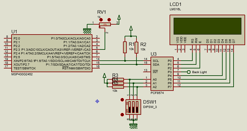
Explanation
In the last example, the ADC channels that were scanned were in an order. Here, however, the story is different but the concept is the same.

Note that all channels are enabled since the topmost channel we have measured here is the Measure VCC channel but intentionally the memory block size is set 1 instead of 12 and only one external channel is enabled. Well, there are some proof-of-concepts to show. The first proof-of-concept is the fact that since we have to set memory block size and memory pointer on our own in the initialization code, it doesn’t matter what these values are in Grace. Secondly, only external channel A3 is sensed since its external I/O is enabled. The rest of the external channels are ignored. This is why A0 reads floating values when the code runs because its external I/O to ADC is disconnected and furthermore it is used to blink the onboard Launchpad LED connected with it. Channel A10 (internal temperature sensor) and A11 (internal VCC sensor) are internal channels and so are not dependent on external I/Os. These channels read as they should. Despite scanning all channels, we can decide which ones we need. Here I demoed sensing channels A0, A3, A10 and A11. Note that these channels are out of a regular or orderly sequence, hence the name of the topic Sensing Multiple Out-of-Sequence ADC10 Channels with DMA.
Demo

Capacitive Touch Overview
Capacitive touch sensing technology is nothing new at present. Cell phones, smartwatches, tablets, portable music players, and even many home appliances that you can name no longer have mechanical touch keys/switches/buttons/variables. All such switching elements have been replaced by more smart and elegant capacitive touch sensors. At present due to this trend even the tiniest new generation microcontroller has capacitive touch sensing capability. When it comes to TI micros, this trend seems to explode to a whole new level.
I haven’t seen so far, any TI MCU without capacitive touch feature. Almost all digital I/Os can be used for capacitive touch as there is no specific dedicated I/Os for such implementations. This makes capacitive touch sensing easy in terms of hardware design. Designing capacitive touch sensors is another story.

In MSP430s, capacitive touch sensing requires two separate timers. These timers create independent time bases and these time bases are compared against each other. One of these time bases is fixed while the other is dependent of the value of touch sensor’s capacitance. When a touch is detected, capacitance changes. This creates a significant difference between the time bases which otherwise remains fairly constant. This is how a touch is detected. This is also a mean to measure capacitance other than touch sensing.
For making all these tasks simple and for rapid development, TI has provided a dedicated Hardware Abstraction Layer (HAL) library for capacitive touch sensing. Use TI’s Resource Explorer to download code examples and library files. Programmer’s Guide SLAA490D discusses implementation of capacitive touch sensing in terms of coding, hardware combinations and others. This page is also an equally important one. Apart from these, there are good literatures from TI that discuss tons of valuable info about capacitive touch sensing technology – from hardware designs to implementation methods.
TI discusses about three methods with which capacitive touch sensing can be achieved. These methods are as follows:
Relaxation Oscillator (RO)
This method counts the number of relaxation oscillator cycles within a fixed period called gate time. Usually for the Value-Line Devices (VLD), the PinOsc feature is used in this method and the key thing to note here is the fact that no external components like external resistors or capacitors are needed to implement capacitive touch sensors. It is this method that we will be observing in this article as our target devices are VLDs.
Resistor Capacitor (RC)
This method is just the opposite of RO method. In this method, the gate time is variable as it is the representation of capacitance while the oscillator time period is fixed. The fixed time base is connected to an internal MSP430 oscillator like the DCO. The variable time base is connected to a capacitor and resistor network. The time it takes to charge and discharge the capacitor through the resistor is now the gate time. The RC method can be realized with any MSP430.
Fast Relaxation Oscillator (fRO)
This method is similar to the RC method except that the variable gate period is created with a relaxation oscillator instead of the charge and discharge time.
TI’s capacitive touch library documentation also recommends which hardware combination to use for a given family of MSP430 microcontroller. Though these are not mandatory, following these recommended combinations reduces code development time and best performances.
Single-Channel Capacitive Touch
This is the very first capacitive touch example we will look at. Although a single capacitive touch button has very little use in real life, it is good for realizing the mechanism behind this capacitive touch technology. If this example is well understood then everything related to capacitive touch sensing will be realized without any confusion or doubt.
Code Example
structure.h (top part only)
#ifndef CTS_STRUCTURE_H_
#define CTS_STRUCTURE_H_
#include "msp430.h"
#include <stdint.h>
/* Public Globals */
// Middle Element on the LaunchPad Capacitive Touch BoosterPack
extern const struct Element middle_element;
// One Button Sensor
extern const struct Sensor one_button;
//****** RAM ALLOCATION ********************************************************
// TOTAL_NUMBER_OF_ELEMENTS represents the total number of elements used, even if
// they are going to be segmented into seperate groups. This defines the
// RAM allocation for the baseline tracking. If only the TI_CAPT_Raw function
// is used, then this definition should be removed to conserve RAM space.
#define TOTAL_NUMBER_OF_ELEMENTS 1
// If the RAM_FOR_FLASH definition is removed, then the appropriate HEAP size
// must be allocated. 2 bytes * MAXIMUM_NUMBER_OF_ELEMENTS_PER_SENSOR + 2 bytes
// of overhead.
#define RAM_FOR_FLASH
//****** Structure Array Definition ********************************************
// This defines the array size in the sensor strucure. In the event that
// RAM_FOR_FLASH is defined, then this also defines the amount of RAM space
// allocated (global variable) for computations.
#define MAXIMUM_NUMBER_OF_ELEMENTS_PER_SENSOR 1
//****** Choosing a Measurement Method ****************************************
// These variables are references to the definitions found in structure.c and
// must be generated per the application.
// possible values for the method field
// OSCILLATOR DEFINITIONS
//#define RO_COMPAp_TA0_WDTp 64
#define RO_PINOSC_TA0_WDTp 65
. . . .
structure.c
#include "structure.h"
// Middle Element (P2.5)
const struct Element middle_element =
{
.inputPxselRegister = (uint8_t *)&P2SEL,
.inputPxsel2Register = (uint8_t *)&P2SEL2,
.inputBits = BIT4,
// When using an abstracted function to measure the element
// the 100*(maxResponse - threshold) < 0xFFFF
// ie maxResponse - threshold < 655
.maxResponse = (450 + 655),
.threshold = 450
};
// One Button Sensor
const struct Sensor one_button =
{
.halDefinition = RO_PINOSC_TA0_WDTp, // Sensing Method
.numElements = 1, // # of Elements
.baseOffset = 0, // First element index = 0
// Pointer to elements
.arrayPtr[0] = &middle_element, // point to middle element
// Timer Information
.measGateSource= GATE_WDT_ACLK, // 0->SMCLK, 1-> ACLK
.accumulationCycles= WDTp_GATE_64 //64 - Default
};
main.c
#include <msp430.h>
#include "CTS_Layer.h"
#include "CTS_HAL.h"
#include "structure.h"
#define DELAY 4000
void GPIO_graceInit(void);
void BCSplus_graceInit(void);
void sleep(unsigned int time);
#pragma vector = TIMER0_A0_VECTOR
__interrupt void ISR_Timer0_A0(void)
{
TA0CTL &= ~MC_1;
TA0CCTL0 &= ~(CCIE);
__bic_SR_register_on_exit(LPM3_bits + GIE);
}
#pragma vector = PORT2_VECTOR, \
PORT1_VECTOR, \
TIMER0_A1_VECTOR, \
USI_VECTOR, \
NMI_VECTOR,COMPARATORA_VECTOR, \
ADC10_VECTOR
__interrupt void ISR_trap(void)
{
// the following will cause an access violation which results in a PUC reset
WDTCTL = 0;
}
// Main Function
void main(void)
{
WDTCTL = WDTPW + WDTHOLD; // Stop watchdog timer
GPIO_graceInit();
BCSplus_graceInit();
TI_CAPT_Init_Baseline(&one_button);
TI_CAPT_Update_Baseline(&one_button, 6);
while (1)
{
if(TI_CAPT_Button(&one_button))
{
P1OUT ^= BIT0;
P1OUT |= BIT6;
}
else
{
P1OUT &= ~BIT6;
}
sleep(DELAY);
}
} // End Main
void GPIO_graceInit(void)
{
/* USER CODE START (section: GPIO_graceInit_prologue) */
/* User initialization code */
/* USER CODE END (section: GPIO_graceInit_prologue) */
/* Port 1 Output Register */
P1OUT = 0;
/* Port 1 Direction Register */
P1DIR = BIT0 | BIT6;
/* Port 1 Interrupt Edge Select Register */
P1IES = 0;
/* Port 1 Interrupt Flag Register */
P1IFG = 0;
/* Port 2 Output Register */
P2OUT = 0;
/* Port 2 Port Select Register */
P2SEL &= ~(BIT6 | BIT7);
/* Port 2 Direction Register */
P2DIR = 0;
/* Port 2 Interrupt Edge Select Register */
P2IES = 0;
/* Port 2 Interrupt Flag Register */
P2IFG = 0;
/* USER CODE START (section: GPIO_graceInit_epilogue) */
/* User code */
/* USER CODE END (section: GPIO_graceInit_epilogue) */
}
void BCSplus_graceInit(void)
{
/* USER CODE START (section: BCSplus_graceInit_prologue) */
/* User initialization code */
/* USER CODE END (section: BCSplus_graceInit_prologue) */
/*
* Basic Clock System Control 2
*
* SELM_0 -- DCOCLK
* DIVM_0 -- Divide by 1
* ~SELS -- DCOCLK
* DIVS_3 -- Divide by 8
* ~DCOR -- DCO uses internal resistor
*
* Note: ~<BIT> indicates that <BIT> has value zero
*/
BCSCTL2 = SELM_0 | DIVM_0 | DIVS_3;
if (CALBC1_12MHZ != 0xFF) {
/* Adjust this accordingly to your VCC rise time */
__delay_cycles(100000);
/* Follow recommended flow. First, clear all DCOx and MODx bits. Then
* apply new RSELx values. Finally, apply new DCOx and MODx bit values.
*/
DCOCTL = 0x00;
BCSCTL1 = CALBC1_12MHZ; /* Set DCO to 12MHz */
DCOCTL = CALDCO_12MHZ;
}
/*
* Basic Clock System Control 1
*
* XT2OFF -- Disable XT2CLK
* ~XTS -- Low Frequency
* DIVA_0 -- Divide by 1
*
* Note: ~XTS indicates that XTS has value zero
*/
BCSCTL1 |= XT2OFF | DIVA_0;
/*
* Basic Clock System Control 3
*
* XT2S_0 -- 0.4 - 1 MHz
* LFXT1S_2 -- If XTS = 0, XT1 = VLOCLK ; If XTS = 1, XT1 = 3 - 16-MHz crystal or resonator
* XCAP_1 -- ~6 pF
*/
BCSCTL3 = XT2S_0 | LFXT1S_2 | XCAP_1;
/* USER CODE START (section: BCSplus_graceInit_epilogue) */
/* User code */
/* USER CODE END (section: BCSplus_graceInit_epilogue) */
}
void sleep(unsigned int time)
{
TA0CCR0 = time;
TA0CTL = TASSEL_1 | ID_0 | MC_1 | TACLR;
TA0CCTL0 &= ~CCIFG;
TA0CCTL0 |= CCIE;
__bis_SR_register(LPM3_bits+GIE);
__no_operation();
}
Simulation
Capacitive touch sensing cannot be simulated in software like Proteus VSM.
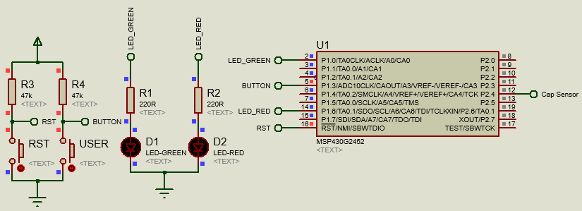
Explanation
In Grace, there is no option to generate configuration for capacitive touch. However, MSP430Ware demos some examples for such. It is better to use the examples given there for project start up. I did the same. However, for a beginner it is must to which things to modify and why do so. Implementing capacitive touch requires three pairs of TI’s HAL library files. These are as follows and are needed to be integrated with your project:
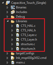
Of these files, the important files that are needed to be edited to set capacitive touch properties of capacitive touch sensor(s) are the structure header and source files. The rest two pairs of files should be left untouched.
In the structure header file, external constant structure named middle_element defines I/O port(s) properties of capacitive sensor(s). Similarly, one_button defines timer/watchdog properties. These two external structures have other functions too. We will see these properties when will discuss the source file. Next, we have to define how many capacitive touch sensors are there in our design. Finally, we have to set which hardware combination to use. In our case, Timer0_A, watchdog timer and digital I/O’s PinOsc functionality are used to implement capacitive touch. The rest of the file is not needed to be changed anywhere.
// Middle Element on the LaunchPad Capacitive Touch BoosterPack
extern const struct Element middle_element;
// One Button Sensor
extern const struct Sensor one_button;
//****** RAM ALLOCATION ********************************************************
// TOTAL_NUMBER_OF_ELEMENTS represents the total number of elements used, even if
// they are going to be segmented into seperate groups. This defines the
// RAM allocation for the baseline tracking. If only the TI_CAPT_Raw function
// is used, then this definition should be removed to conserve RAM space.
#define TOTAL_NUMBER_OF_ELEMENTS 1
// If the RAM_FOR_FLASH definition is removed, then the appropriate HEAP size
// must be allocated. 2 bytes * MAXIMUM_NUMBER_OF_ELEMENTS_PER_SENSOR + 2 bytes
// of overhead.
#define RAM_FOR_FLASH
//****** Structure Array Definition ********************************************
// This defines the array size in the sensor strucure. In the event that
// RAM_FOR_FLASH is defined, then this also defines the amount of RAM space
// allocated (global variable) for computations.
#define MAXIMUM_NUMBER_OF_ELEMENTS_PER_SENSOR 1
//****** Choosing a Measurement Method ****************************************
// These variables are references to the definitions found in structure.c and
// must be generated per the application.
// possible values for the method field
// OSCILLATOR DEFINITIONS
//#define RO_COMPAp_TA0_WDTp 64
#define RO_PINOSC_TA0_WDTp 65
Now it is time to explain the structure source file.
const struct Element middle_element =
{
.inputPxselRegister = (uint8_t *)&P2SEL,
.inputPxsel2Register = (uint8_t *)&P2SEL2,
.inputBits = BIT4,
// When using an abstracted function to measure the element
// the 100*(maxResponse - threshold) < 0xFFFF
// ie maxResponse - threshold < 655
.maxResponse = (450 + 655),
.threshold = 450
};
PxSEL and PxSEL2 bits internally set PinOsc feature. Since this example demonstrated one capacitive touch button only one element is connected to BIT4 of port P2. Optionally, we can set the threshold limit on which we can positively identify a touch.
// One Button Sensor
const struct Sensor one_button =
{
.halDefinition = RO_PINOSC_TA0_WDTp, // Sensing Method
.numElements = 1, // # of Elements
.baseOffset = 0, // First element index = 0
// Pointer to elements
.arrayPtr[0] = &middle_element, // point to middle element
// Timer Information
.measGateSource= GATE_WDT_ACLK, // 0->SMCLK, 1-> ACLK
.accumulationCycles= WDTp_GATE_64 //64 - Default
};
The second part of the source file details which method is used along with the name and number of element(s) to sense. Basically, here we have nothing to do other than to let this part know the structure name of our element(s) and the number of sensors.
#pragma vector = TIMER0_A0_VECTOR
__interrupt void ISR_Timer0_A0(void)
{
TA0CTL &= ~MC_1;
TA0CCTL0 &= ~(CCIE);
__bic_SR_register_on_exit(LPM3_bits + GIE);
}
#pragma vector = PORT2_VECTOR, \
PORT1_VECTOR, \
TIMER0_A1_VECTOR, \
USI_VECTOR, \
NMI_VECTOR,COMPARATORA_VECTOR, \
ADC10_VECTOR
__interrupt void ISR_trap(void)
{
// the following will cause an access violation which results in a PUC reset
WDTCTL = 0;
}
Two interrupts are needed to be called. The first is the Timer0_A ISR. This acts like a wakeup alarm. Once the capacitive sensing and other tasks in the main loop are completed, this timer is started and low power mode is entered. After timeout, this timer interrupts causing the main tasks to reoccur and leave low power mode momentarily. The second is a Trap ISR. Trap ISR ensures that if for some reason something happens that you didn’t expect it will reset the MCU. The interrupt vectors assigned here are those vectors which we won’t be using. If any of these pop-up, a reset will occur.
void main(void)
{
WDTCTL = WDTPW + WDTHOLD; // Stop watchdog timer
GPIO_graceInit();
BCSplus_graceInit();
TI_CAPT_Init_Baseline(&one_button);
TI_CAPT_Update_Baseline(&one_button, 6);
while (1)
{
if(TI_CAPT_Button(&one_button))
{
P1OUT ^= BIT0;
P1OUT |= BIT6;
}
else
{
P1OUT &= ~BIT6;
}
sleep(DELAY);
}
}
The main function is perhaps the smallest one here. Except for the other parts with which by now we are familiar, there are a few new lines of code. Just before the main loop, the two lines of code right above it, initialize the capacitive touch sensor. Number 6 in the function TI_CAPT_Update_Baseline states the number of samples to capture for accurately sensing a touch. If a valid touch is detected, the LEDs of Launchpad board are toggled.
Demo
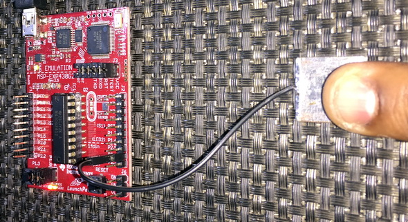
Multi-Channel Capacitive Touch
Unlike single capacitive touch buttons, multiple capacitive sensors have several potential uses. These include multi-touch buttons, sliders, wheels, rotary encoders, etc. Here we will have a look at multiple capacitive touch buttons and the example demonstrated here is basically the extension of the last one. However, for multi-touch capacitive touch sensors, there are twists in the software end apart from hardware design and considerations.

Code Example
structure.h (top part only)
#ifndef CTS_STRUCTURE_H_
#define CTS_STRUCTURE_H_
#include "msp430.h"
#include <stdint.h>
/* Public Globals */
extern const struct Element middle_element;
extern const struct Element up_element;
extern const struct Element down_element;
// Identify all sensors defined in structure.c
extern const struct Sensor multi_buttons;
//****** RAM ALLOCATION ********************************************************
// TOTAL_NUMBER_OF_ELEMENTS represents the total number of elements used, even if
// they are going to be segmented into seperate groups. This defines the
// RAM allocation for the baseline tracking. If only the TI_CAPT_Raw function
// is used, then this definition should be removed to conserve RAM space.
#define TOTAL_NUMBER_OF_ELEMENTS 3
// If the RAM_FOR_FLASH definition is removed, then the appropriate HEAP size
// must be allocated. 2 bytes * MAXIMUM_NUMBER_OF_ELEMENTS_PER_SENSOR + 2 bytes
// of overhead.
#define RAM_FOR_FLASH
//****** Structure Array Definition ********************************************
// This defines the array size in the sensor strucure. In the event that
// RAM_FOR_FLASH is defined, then this also defines the amount of RAM space
// allocated (global variable) for computations.
#define MAXIMUM_NUMBER_OF_ELEMENTS_PER_SENSOR 3
//****** Choosing a Measurement Method ****************************************
// These variables are references to the definitions found in structure.c and
// must be generated per the application.
// possible values for the method field
// OSCILLATOR DEFINITIONS
//#define RO_COMPAp_TA0_WDTp 64
#define RO_PINOSC_TA0_WDTp 65
. . . .
structure.c
#include "structure.h"
// Middle Element (P2.5)
const struct Element middle_element = {
.inputPxselRegister = (unsigned char *)&P2SEL,
.inputPxsel2Register = (unsigned char *)&P2SEL2,
.inputBits = BIT5,
// When using an abstracted function to measure the element
// the 100*(maxResponse - threshold) < 0xFFFF
// ie maxResponse - threshold < 655
.maxResponse = (100 + 655),
.threshold = 100
};
// Up Element (P2.4)
const struct Element up_element = {
.inputPxselRegister = (unsigned char *)&P2SEL,
.inputPxsel2Register = (unsigned char *)&P2SEL2,
.inputBits = BIT4,
// When using an abstracted function to measure the element
// the 100*(maxResponse - threshold) < 0xFFFF
// ie maxResponse - threshold < 655
.maxResponse = (100 + 655),
.threshold = 100
};
// Down Element (P2.3)
const struct Element down_element =
{
.inputPxselRegister = (unsigned char *)&P2SEL,
.inputPxsel2Register = (unsigned char *)&P2SEL2,
.inputBits = BIT3,
// When using an abstracted function to measure the element
// the 100*(maxResponse - threshold) < 0xFFFF
// ie maxResponse - threshold < 655
.maxResponse = (100 + 655),
.threshold = 100
};
//*** CAP TOUCH HANDLER *******************************************************/
// This defines the grouping of sensors, the method to measure change in
// capacitance, and the function of the group
const struct Sensor multi_buttons =
{
.halDefinition = RO_PINOSC_TA0_WDTp,
.numElements = 3,
.baseOffset = 0,
// Pointer to elements
.arrayPtr[0] = &up_element, // point to up element
.arrayPtr[1] = &down_element, // point to down element
.arrayPtr[2] = &middle_element, // point to middle element
// Timer Information
.measGateSource= GATE_WDT_ACLK, // 0->SMCLK, 1-> ACLK
.accumulationCycles= WDTp_GATE_64 //64 - Default
};
main.c
#include <msp430.h>
#include "CTS_Layer.h"
#include "CTS_HAL.h"
#include "structure.h"
#define DELAY 4000
struct Element * keyPressed;
void GPIO_graceInit(void);
void BCSplus_graceInit(void);
void sleep(unsigned int time);
#pragma vector = TIMER0_A0_VECTOR
__interrupt void ISR_Timer0_A0(void)
{
TA0CTL &= ~MC_1;
TA0CCTL0 &= ~(CCIE);
__bic_SR_register_on_exit(LPM3_bits + GIE);
}
#pragma vector = PORT2_VECTOR, \
PORT1_VECTOR, \
TIMER0_A1_VECTOR, \
USI_VECTOR, \
NMI_VECTOR,COMPARATORA_VECTOR, \
ADC10_VECTOR
__interrupt void ISR_trap(void)
{
// the following will cause an access violation which results in a PUC reset
WDTCTL = 0;
}
// Main Function
void main(void)
{
WDTCTL = WDTPW + WDTHOLD; // Stop watchdog timer
GPIO_graceInit();
BCSplus_graceInit();
TI_CAPT_Init_Baseline(&multi_buttons);
TI_CAPT_Update_Baseline(&multi_buttons, 25);
// Main loop starts here
while (1)
{
keyPressed = (struct Element *)TI_CAPT_Buttons(&multi_buttons);
if(keyPressed)
{
// Up Element
if(keyPressed == &up_element)
{
P1OUT |= BIT0;
}
// Down Element
if(keyPressed == &down_element)
{
P1OUT |= BIT6;
}
// Middle Element
if(keyPressed == &middle_element)
{
P1OUT = 0;
}
}
sleep(DELAY);
}
} // End Main
void GPIO_graceInit(void)
{
/* USER CODE START (section: GPIO_graceInit_prologue) */
/* User initialization code */
/* USER CODE END (section: GPIO_graceInit_prologue) */
/* Port 1 Output Register */
P1OUT = 0;
/* Port 1 Direction Register */
P1DIR = BIT0 | BIT6;
/* Port 1 Interrupt Edge Select Register */
P1IES = 0;
/* Port 1 Interrupt Flag Register */
P1IFG = 0;
/* Port 2 Output Register */
P2OUT = 0;
/* Port 2 Port Select Register */
P2SEL &= ~(BIT6 | BIT7);
/* Port 2 Direction Register */
P2DIR = 0;
/* Port 2 Interrupt Edge Select Register */
P2IES = 0;
/* Port 2 Interrupt Flag Register */
P2IFG = 0;
/* USER CODE START (section: GPIO_graceInit_epilogue) */
/* User code */
/* USER CODE END (section: GPIO_graceInit_epilogue) */
}
void BCSplus_graceInit(void)
{
/* USER CODE START (section: BCSplus_graceInit_prologue) */
/* User initialization code */
/* USER CODE END (section: BCSplus_graceInit_prologue) */
/*
* Basic Clock System Control 2
*
* SELM_0 -- DCOCLK
* DIVM_0 -- Divide by 1
* ~SELS -- DCOCLK
* DIVS_0 -- Divide by 1
* ~DCOR -- DCO uses internal resistor
*
* Note: ~<BIT> indicates that <BIT> has value zero
*/
BCSCTL2 = SELM_0 | DIVM_0 | DIVS_0;
if (CALBC1_8MHZ != 0xFF)
{
/* Adjust this accordingly to your VCC rise time */
__delay_cycles(100000);
// Follow recommended flow. First, clear all DCOx and MODx bits. Then
// apply new RSELx values. Finally, apply new DCOx and MODx bit values.
DCOCTL = 0x00;
BCSCTL1 = CALBC1_8MHZ; /* Set DCO to 8MHz */
DCOCTL = CALDCO_8MHZ;
}
/*
* Basic Clock System Control 1
*
* XT2OFF -- Disable XT2CLK
* ~XTS -- Low Frequency
* DIVA_0 -- Divide by 1
*
* Note: ~XTS indicates that XTS has value zero
*/
BCSCTL1 |= XT2OFF | DIVA_0;
/*
* Basic Clock System Control 3
*
* XT2S_0 -- 0.4 - 1 MHz
* LFXT1S_2 -- If XTS = 0, XT1 = VLOCLK ; If XTS = 1, XT1 = 3 - 16-MHz crystal or resonator
* XCAP_1 -- ~6 pF
*/
BCSCTL3 = XT2S_0 | LFXT1S_2 | XCAP_1;
/* USER CODE START (section: BCSplus_graceInit_epilogue) */
/* User code */
/* USER CODE END (section: BCSplus_graceInit_epilogue) */
}
void sleep(unsigned int time)
{
TA0CCR0 = time;
TA0CTL = TASSEL_1 | ID_0 | MC_1 | TACLR;
TA0CCTL0 &= ~CCIFG;
TA0CCTL0 |= CCIE;
__bis_SR_register(LPM3_bits + GIE);
__no_operation();
}
Simulation
Capacitive touch sensing cannot be simulated in software like Proteus VSM.

Explanation
This example uses the same ideas as in the previous example. The header file is slightly modified. Three sensor elements are used and so the number of sensor is set 3. The elements are named differently since each are independent of the other.
extern const struct Element middle_element;
extern const struct Element up_element;
extern const struct Element down_element;
// Identify all sensors defined in structure.c
extern const struct Sensor multi_buttons;
//****** RAM ALLOCATION ********************************************************
// TOTAL_NUMBER_OF_ELEMENTS represents the total number of elements used, even if
// they are going to be segmented into seperate groups. This defines the
// RAM allocation for the baseline tracking. If only the TI_CAPT_Raw function
// is used, then this definition should be removed to conserve RAM space.
#define TOTAL_NUMBER_OF_ELEMENTS 3
....
//****** Structure Array Definition ********************************************
// This defines the array size in the sensor strucure. In the event that
// RAM_FOR_FLASH is defined, then this also defines the amount of RAM space
// allocated (global variable) for computations.
#define MAXIMUM_NUMBER_OF_ELEMENTS_PER_SENSOR 3
The main difference is present in the structure source file. The three different elements are declared independently despite being in the same port. This is so because we need to identify them when a touch is detected.
const struct Element middle_element = {
.inputPxselRegister = (unsigned char *)&P2SEL,
.inputPxsel2Register = (unsigned char *)&P2SEL2,
.inputBits = BIT5,
// When using an abstracted function to measure the element
// the 100*(maxResponse - threshold) < 0xFFFF
// ie maxResponse - threshold < 655
.maxResponse = (100 + 655),
.threshold = 100
};
// Up Element (P2.4)
const struct Element up_element = {
.inputPxselRegister = (unsigned char *)&P2SEL,
.inputPxsel2Register = (unsigned char *)&P2SEL2,
.inputBits = BIT4,
// When using an abstracted function to measure the element
// the 100*(maxResponse - threshold) < 0xFFFF
// ie maxResponse - threshold < 655
.maxResponse = (100 + 655),
.threshold = 100
};
// Down Element (P2.3)
const struct Element down_element =
{
.inputPxselRegister = (unsigned char *)&P2SEL,
.inputPxsel2Register = (unsigned char *)&P2SEL2,
.inputBits = BIT3,
// When using an abstracted function to measure the element
// the 100*(maxResponse - threshold) < 0xFFFF
// ie maxResponse - threshold < 655
.maxResponse = (100 + 655),
.threshold = 100
};
//*** CAP TOUCH HANDLER *******************************************************/
// This defines the grouping of sensors, the method to measure change in
// capacitance, and the function of the group
const struct Sensor multi_buttons =
{
.halDefinition = RO_PINOSC_TA0_WDTp,
.numElements = 3,
.baseOffset = 0,
// Pointer to elements
.arrayPtr[0] = &up_element, // point to up element
.arrayPtr[1] = &down_element, // point to down element
.arrayPtr[2] = &middle_element, // point to middle element
// Timer Information
.measGateSource= GATE_WDT_ACLK, // 0->SMCLK, 1-> ACLK
.accumulationCycles= WDTp_GATE_64 //64 - Default
};
Similarly, the sensor structure is also modified for these three elements. The main code is almost identical to the single sensor demo. However, the variable keyPressed is used to check which element was touched. According to touch on different element states of Launchpad board LEDs are altered.
keyPressed = (struct Element *)TI_CAPT_Buttons(&multi_buttons);
if(keyPressed)
{
// Up Element
if(keyPressed == &up_element)
{
P1OUT |= BIT0;
}
// Down Element
if(keyPressed == &down_element)
{
P1OUT |= BIT6;
}
// Middle Element
if(keyPressed == &middle_element)
{
P1OUT = 0;
}
}
Demo

A Brief Intro of MSP430F5529LP Launchpad and TI’s Driver Library
Up till now we have seen and used the power of Grace configuration tool, MSP430G2xxx devices and only mentioned the name Driver Library. At present for micros with too many hardware resources, it is really very difficult to go through their individual datasheet line-by-line and memorize register names and their purposes. However, we just need peripheral initialization once in a code and it should not take much of a project’s development time. Likewise, when moving from one micro sub family to another or just interchanging devices within a given family, there should be some similarity in coding and hardware or else it be really very much difficult to keep track of everything. To overcome such issues and many others, mainstream embedded system solution manufacturers like TI offer different code development solutions ranging from graphical tools like Grace to code examples/templates as in TI’s Resource Explorer. The Peripheral Driver Library or simply DriverLib is one solution that somewhat resides between aforementioned two. It is a set of drivers for accessing the peripherals found on MSP430 micros and is similar to HAL libraries used for ARM micros. So far, we have not used this library pack as it doesn’t support VLDs. Details of TI’s driver library can be found here. Please have it downloaded as we will need it for the demo.
As mentioned before, there are other more resourceful and powerful MSP430s and the driver library is intended for such robust devices. MSP430F5529LP is one such powerful device. It is a microcontroller mainly intended for USB application development and has 128kB of flash and 8kB RAM. There is an inexpensive Launchpad board dedicated for this awesome micro and it delivers the punch needed in complex big projects. Details of this Launchpad board can be found here.
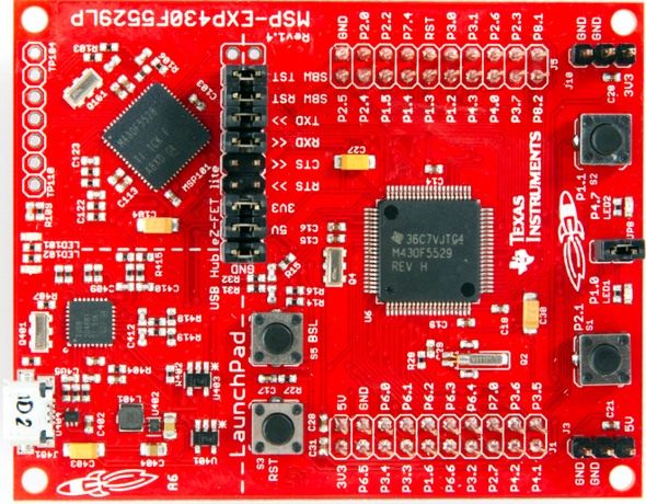
In this final section, we will briefly see the potential of combining TI’s Driver Library with MSP430F5529LP.
How tos?
Google and download the Energia pinmap for MSP430F5529LP.
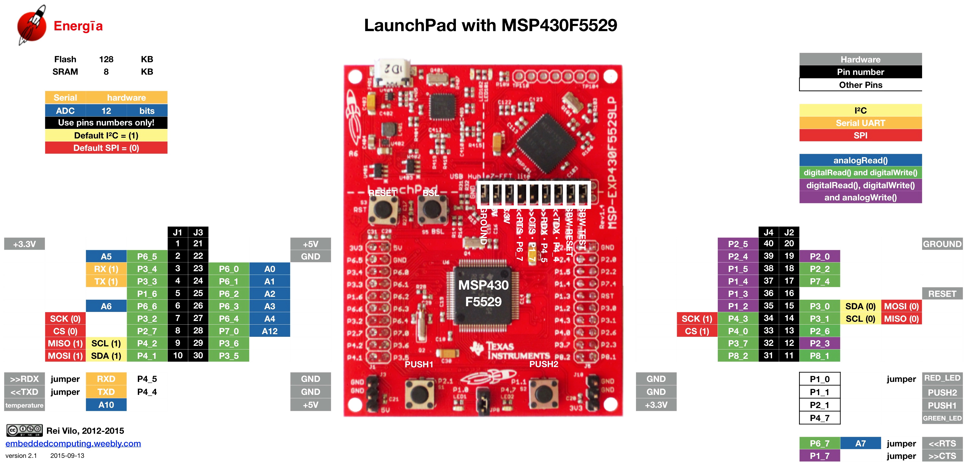
I assume that by now you have downloaded the latest version of DriverLib and other documentations regarding this and the MSP430F5529LP Launchpad board.
Extract the DriverLib zip file and copy the correct DriverLib folder (MSP430F5xx_6xx folder in our case) to your project folder. In my case, I copied this folder and renamed it as driverlib. The process is same as what we did for our own-built library files.
Let the compiler know the physical paths of this folder just like the custom library files. Rest of the works is same as before.
Code Example
#include "driverlib.h"
#include "delay.h"
void main(void)
{
unsigned char s = 0x00;
WDT_A_hold(WDT_A_BASE);
GPIO_setAsOutputPin (GPIO_PORT_P1, GPIO_PIN0);
GPIO_setDriveStrength(GPIO_PORT_P1, GPIO_PIN0, GPIO_FULL_OUTPUT_DRIVE_STRENGTH);
GPIO_setAsOutputPin (GPIO_PORT_P4, GPIO_PIN7);
GPIO_setDriveStrength(GPIO_PORT_P4, GPIO_PIN7, GPIO_FULL_OUTPUT_DRIVE_STRENGTH);
GPIO_setAsInputPinWithPullUpResistor(GPIO_PORT_P2, GPIO_PIN1);
GPIO_setAsPeripheralModuleFunctionInputPin(GPIO_PORT_P5, (GPIO_PIN2 | GPIO_PIN4));
GPIO_setAsPeripheralModuleFunctionOutputPin(GPIO_PORT_P5, (GPIO_PIN2 | GPIO_PIN4));
UCS_setExternalClockSource(32768, 4000000);
UCS_turnOnXT2(UCS_XT2_DRIVE_4MHZ_8MHZ);
UCS_turnOnLFXT1(UCS_XT1_DRIVE_0, UCS_XCAP_3);
UCS_initClockSignal(UCS_MCLK, UCS_XT2CLK_SELECT, UCS_CLOCK_DIVIDER_1);
UCS_initClockSignal(UCS_SMCLK, UCS_XT2CLK_SELECT, UCS_CLOCK_DIVIDER_1);
UCS_initClockSignal(UCS_ACLK, UCS_XT1CLK_SELECT, UCS_CLOCK_DIVIDER_1);
while(1)
{
if(GPIO_getInputPinValue(GPIO_PORT_P2, GPIO_PIN1) == false)
{
while(GPIO_getInputPinValue(GPIO_PORT_P2, GPIO_PIN1) == false);
GPIO_setOutputHighOnPin(GPIO_PORT_P1, GPIO_PIN0);
delay_ms(100);
GPIO_setOutputLowOnPin(GPIO_PORT_P1, GPIO_PIN0);
s = ~s;
}
P4OUT ^= BIT7;
switch(s)
{
case 0:
{
delay_ms(100);
break;
}
default:
{
delay_ms(600);
break;
}
}
};
}
Explanation
To keep things simple, I demoed another LED blinking code. Notice that with inclusion of driverlib, everything has changed with meaningful functions. Take the setting of watchdog timer as an example.
WDTCTL = WDTPW | WDTHOLD; //Register-level access
WDT_A_hold(WDT_A_BASE); //DriverLib function call
Instead of setting registers, driverlib functions are just taking some function argument(s) to set desired pin according to our wish. The functions and the arguments have meaningful names instead of magical numbers. This way of coding gives a fast overview of our code and the development time and efforts are greatly reduced. All register-level tasks are done under the hood of driverlib. This doesn’t however restrict us from going the old-fashioned way of using register-based coding. Still it is possible:
P4OUT ^= BIT7;
The code begins with GPIO settings as follows:
GPIO_setAsOutputPin (GPIO_PORT_P1, GPIO_PIN0);
GPIO_setDriveStrength(GPIO_PORT_P1, GPIO_PIN0, GPIO_FULL_OUTPUT_DRIVE_STRENGTH);
GPIO_setAsOutputPin (GPIO_PORT_P4, GPIO_PIN7);
GPIO_setDriveStrength(GPIO_PORT_P4, GPIO_PIN7, GPIO_FULL_OUTPUT_DRIVE_STRENGTH);
GPIO_setAsInputPinWithPullUpResistor(GPIO_PORT_P2, GPIO_PIN1);
GPIO_setAsPeripheralModuleFunctionInputPin(GPIO_PORT_P5, (GPIO_PIN2 | GPIO_PIN4));
GPIO_setAsPeripheralModuleFunctionOutputPin(GPIO_PORT_P5, (GPIO_PIN2 | GPIO_PIN4));
Two pins P1_0 and P4_7 are set as outputs with full drive strength since these pins have LEDs connected with them. P2_1 is set as an input with pull-up as it is connected with an onboard push button. Some pins of P5 are set for peripheral modules because these pins are connected with external crystals.
Next, we set to configure the clock system. There are two onboard external crystals – one 32.768kHz clock crystal and one 4MHz crystal. UCS stands for Unified Clock System. Like the basic clock system in MSP430G2xxx devices, this a complex network of clock system with lot of options. There are several internal and external clock sources to clock the main clock, the sub-main clock and the auxiliary clock signals. Here, I used the external crystal clocks to clock MCLK, SMCLK and ACLK
UCS_setExternalClockSource(32768, 4000000);
UCS_turnOnXT2(UCS_XT2_DRIVE_4MHZ_8MHZ);
UCS_turnOnLFXT1(UCS_XT1_DRIVE_0, UCS_XCAP_3);
UCS_initClockSignal(UCS_MCLK, UCS_XT2CLK_SELECT, UCS_CLOCK_DIVIDER_1);
UCS_initClockSignal(UCS_SMCLK, UCS_XT2CLK_SELECT, UCS_CLOCK_DIVIDER_1);
UCS_initClockSignal(UCS_ACLK, UCS_XT1CLK_SELECT, UCS_CLOCK_DIVIDER_1);
In the main loop, the Launchpad’s green LED (P4_7) is toggled at a given flash rate. When the onboard user push button (P2_1) is pressed, the onboard red LED (P1_0) is briefly turned on and the rate of green LED’s flashing is altered.
if(GPIO_getInputPinValue(GPIO_PORT_P2, GPIO_PIN1) == false)
{
while(GPIO_getInputPinValue(GPIO_PORT_P2, GPIO_PIN1) == false);
GPIO_setOutputHighOnPin(GPIO_PORT_P1, GPIO_PIN0);
delay_ms(100);
GPIO_setOutputLowOnPin(GPIO_PORT_P1, GPIO_PIN0);
s = ~s;
}
P4OUT ^= BIT7;
switch(s)
{
case 0:
{
delay_ms(100);
break;
}
default:
{
delay_ms(600);
break;
}
}
Demo
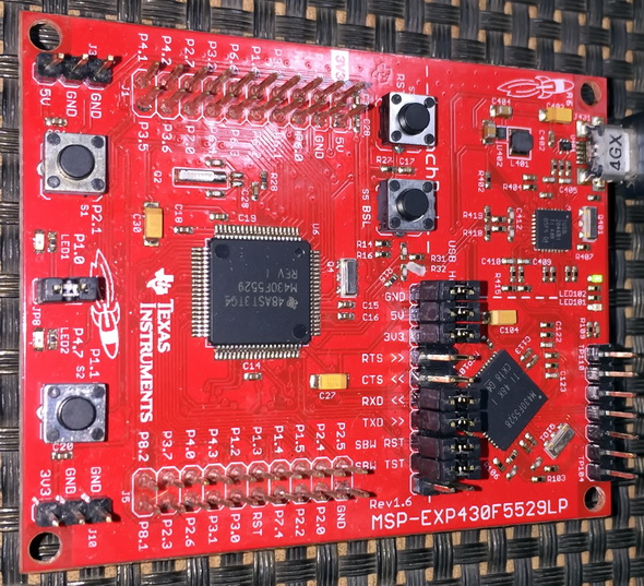
All code examples and this documentation is available for download from here.
Happy coding.
Author: Shawon M. Shahryiar
https://www.facebook.com/groups/microarena
https://www.facebook.com/MicroArena 31.03.2018
** Some images have been taken from the documents and webpages of Texas Instruments (TI) and Mikroelektronika.
|
|
Can you share the Fonts.h file for the OLED interface
All stuffs have been shared here in my github….
https://github.com/sshahryiar/MSP430G2xxx-Tutorial
Good day Shawon
Just awesome again!! Thank you very much for the time you have put aside to write these articles and share it with newcomers like me. Thank you so much for making it available in pdf format and providing us with the code examples.
It is great to work with real life, practical applications.
It is greatly appreciated!!
Regards from South Africa
Start to be interested in TI MSP430s I have found your articles … amazing source of information, thank you very much.