Tag Archives: STM32


STM32 GPIO Ports Insights

In any microcontroller there is at least one general purpose input-output port. STM32 is a not different breed and as expected it also has several GPIO ports. These ports are usually named GPIOA, GPIOB, etc. but unlike most 8/16-bit micros these ports are 16 bit wide. Thus, in general, every port has 16 IO pins. Port pins have several modes of operation and this is what that makes them both robust and complex at first. In development boards the IO port pin naming is cut short and so we’ll find PA0, PB12, etc. instead of GPIOA0, GPIOB12, etc. Even in the reference manuals this short naming is used widely. In the end every I/O pin is general purpose in nature.

Key points with STM32’s GPIO

  • Upon any reset event all GPIOs are floating inputs. This prevents any accidental damage to GPIOs in the event of emergency.
  • All GPIO registers are needed to be accessed with 32 bit words. This is mandatory.
  • Reserved bits for any GPIO register are kept at reset values i.e. 0.
  • For every GPIO port there are seven registers but the only the first four are the most important ones. The rest can be ignored most of the times.
  • These important GPIO registers per port are CRL, CRH, IDR and ODR. The rest three registers for GPIO ports can be avoided at the beginning.
  • For bit set and for bit clear, operations REGx |= (1 << bit) and REGx &= ~ (1 << bit) respectively are very handy and efficient. However MikroC compiler provides bit level access though its internal header file coding like this GPIOB_BSRRbits.BS15. We can use this method or the other one.
  • Some IOs are 5V tolerant and are label “FT” in datasheets and other docs. The rest of the I/O pins are not that tolerant and so 3.3V operation should always be ensured. STM32 has a maximum VDD tolerance of 4V but this value shouldn’t be used in any situation for safe operation. Best is to avoid 5V use with GPIOs whenever possible. This will help in avoiding accidental damage to the micro due to common mistakes.
  • Unused GPIO pins should be kept at reset state or tied to ground with 10kΩ resistors so that they remain either as floating inputs or safely connected to ground though it’s not a must.
  • I/O pins can source or sink currents up to 25mA. Thus direct LED drive is possible with them. To drive loads that need more than this value, we must use external BJTs, MOSFETs, optocouplers, transistor arrays or other driver devices.
  • I/O pins should not directly drive inductive or capacitive loads.
  • Care should be taken to avoid driving outputs beyond 50MHz. This is the maximum I/O pin frequency rating.
  • CRL/H registers essential set GPIO pin operating mode independently as according to the table below:

Port Configurations

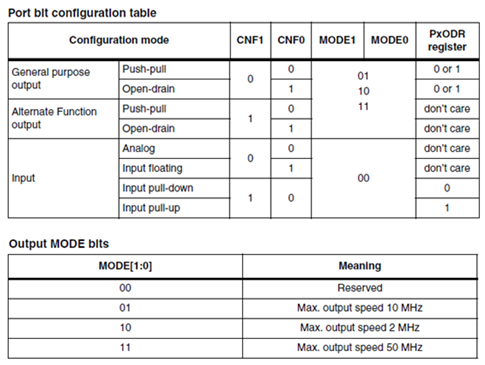
  • CRL sets GPIOs from 0 – 7 while CRH sets from 8 – 15. All IO ports are 16 bit wide unlike common 8 bit micros like PIC or AVR.

Read more

STM32 Programming Tips and Tricks

I remember that once in the beginning I said that I don’t want to buy a programmer/debugger hardware for learning a new MCU like the STM32 and also STM32s already come with built-in bootloader to facilitate programming via USART just like Arduino. Still the second is true. Well what about the first? To my own surprise I actually acquired a number of STM32-related stuffs since the time I started playing and exploring them. I actually bought both ST-Link 1 and 2 programmer-debuggers and several STM32 boards from Waveshare Electronics (http://www.wvshare.com). I believe learning new stuffs is more valuable than anything else.

ST-Link Programmer/Debugger

ST-Link 1 (AKA ST-Link) and ST-Link v2 are both basically the same programmer/debugger hardware with some minor exceptions. ST-Link 2 has 5V tolerance for JTAG interface, it has a bicolour status LED and it also has a separate programming interface for STM8 micros unlike ST-Link 1. There is also an ISOL version of ST-Link2 that galvanically isolates it from its target using optoelectronics.

stlinkgreycablewhite

ST-LINKV2_3

Read more

STM32 Internals

STM32 micros as we know are high-end micros and this high-end tag is not only due to its memory, speed and hardware richness. An advanced micro like this also needs advanced internal supporting hardware. Most of us know about watchdog timers from previous experiences with common 8 bit MCUs like AVR and PIC. However when it comes to STM32 the idea of watchdog circuitry is elaborated. The options available for clock are also enhanced in the STM32 micros. In this post, we will see some of these supporting internal hardware. We will examine the use and operation of two different watchdog timers – Independent Watchdog (IWDG) and Window Watchdog (WWDG), and the clock options usually found in common STM32 micros.

Clock Options

In a robust microcontroller like the STM32 there are several options for clock. At first the whole stuff may look a bit complex. Indeed it is complicated but not too difficult to understand. The simplified block diagram below shows the common clock arrangement inside a STM32F103 series MCU.

Clock Internal

STM32F103 Internal Clock Arrangement (Source: The Insiders Guide to the STM32 ARM based Microcontroller from HITEX, http://www.hitex.com/fileadmin/pdf/insiders-guides/stm32/isg-stm32-v18d-scr.pdf)

Read more

STM32 External Interrupt

In my earlier post on STM32 GPIOs I showed how to flash a LED with variable delay times. That example was based on polling method where the code continuously monitored the logic state of a GPIO input pin attached to a push button to determine the delay amount. Obviously that won’t be an efficient technique when a program will be of a considerable size and complexity. This is simply so because the CPU will have to check the GPIO’s logic state every time the super-loop (while (1) loop in the main function) repeats and the push button will also not be responsive during the software delay function calls. Thus the overall performance is poor and not real-time. To get rid of these issues, we’ll need to use external interrupts – a vital feature in every common microcontroller.

STM32F1xx series are ARM Cortex M3 based MCUs. The Cortex M3 based MCUs have a sophisticated and yet easy to use interrupt system called the Nested Vectored Interrupt Controller (NVIC). It ensures low latency and high performance. There are several features of the NVIC and these are handled by the compiler. Our job is simply to enjoy the lightning fast interrupt responses owing to the NVIC. In many MCUs’ interrupt system, interrupt priority can be set and Reset has the highest interrupt priority over anything else. The same things go for STM32s too. However at present I’m not going to go that deep as that’s not needed for now. In some upcoming post may be I’ll discuss the NVIC in details. As per STM32’s reference manuals for more information on exceptions and NVIC programming read Chapter 5 Exceptions and Chapter 8 Nested Vectored Interrupt Controller of the ARM Cortex-M3 Technical Reference Manual. There are other interrupts that are related to RTC, timer, etc. We won’t also look into them in this post. We will learn about them when we learn about the related hardware with them.

EXTI internal

Read more

STM32 Serial Communication

STM32 micros just like any other micro provide hardware for serial communication. As we all know serial communication is a very important tool for debugging, connecting with external hardware like RFID, GPS, GSM modems, etc. and for performing other communication-related tasks. STM32s have several hardware serial (USART) ports. The number of ports available in a STM32 micro is dependent on device family type and the device itself. Typically there are at least 5 serial ports. Apart from the basic serial communication needs, STM32’s USART hardware also have support for LIN, one-wire, smart card protocols, SPI and IrDA. We can even utilize STM32’s DMA controller with USART hardware to achieve high speed automated data communication. Thus these hardware are truly universal synchronous-asynchronous receiver-transmitters.

In any standard serial communication, we need three wires – TX, RX and GND. TX pin is an output pin and transmits data serially to another device’s RX pin. RX pin is an input pin and is responsible for receiving data from another device’s TX pin. The two devices connected in this way must have same ground (GND). There are other pins like CTS and RTS which are used for hardware flow control. Additionally there’s also another pin called CK. It is transmitter’s clock output and used usually in SPI and other modes.

Depending on package, USART pins are arranged in the following pattern:

BGA100 LQFP100 LQFP48 LQFP64 Pin Name USART/UART
D9 67 29 41 PA8 USART1_CK
C10 70 32 44 PA11 USART1_CTS
B10 71 33 45 PA12 USART1_RTS
C9 68 30 42 PA9 USART1_TX
D10 69 31 43 PA10 USART1_RX
G3 29 14 20 PA4 USART2_CK
G2 23 10 14 PA0 USART2_CTS
H2 24 11 15 PA1 USART2_RTS
J2 25 12 16 PA2 USART2_TX
K2 26 13 17 PA3 USART2_RX
K8 51 25 33 PB12 USART3_CK
J8 52 26 34 PB13 USART3_CTS
H8 53 27 35 PB14 USART3_RTS
J7 47 21 29 PB10 USART3_TX
K7 48 22 30 PB11 USART3_RX
B8 79 52 PC11 UART4_RX
B9 78 51 PC10 UART4_TX
B7 83 54 PD2 UART5_RX
C8 80 53 PC12 UART5_TX

Personally I’m interested in LQFP packages, particularly 48 and 64 packages as they are mostly used in the most common STM32 development boards. I suggest locating USART/UART pins before working with them.

Read more

« Older Entries Recent Entries »