EasyEDA releases a free, online gerber viewer
|
|
EasyEDA is a free, cloud-based EDA application for drawing circuits, running SPICE simulations, designing PCBs, and even placing orders for fabricating PCBs. Now they have released an online Gerber viewing tool to visualize the Gerber files generated by a PCB CAD tool. The tool supports the Gerber RS-274X format, which is an industry-standard image description format for PCBs. The tool receives the Gerber files in a compressed zipped folder and performs a 2-D rendering to generate high-quality images of top and bottom sides of the PCB. The Gerber viewer also runs a simple design check in the background and displays some useful information about your PCB design, such as its dimensions, minimum clearance, copper trace and silkscreen width, etc.
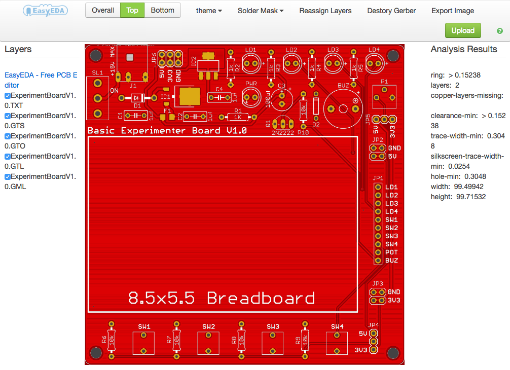
EasyEDA Gerber Viewer tool user interface
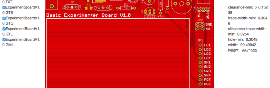
A standalone Gerber viewer like this is a great tool to review the PCB design files before sending them for manufacturing. This tool can be used to verify the component placement and drill holes alignment on the board, as well as to ensure the silkscreen layers are exported correctly in the CAM files. Being on the cloud means it is available to use online at anytime and anywhere, and frees you from having to install any software on your workstation. I am sure this tool will come in handy to the users of EasyEDA for a quick and easy pre-production inspection of their PCB CAD files. At this point, the EasyEDA Gerber Viewer is available at a separate URL. My suggestion to the EasyEDA developer team is to include a link to this tool in the main EasyEDA user interface so that the users can conveniently launch it from there without typing in the URL in a separate browser tab. For a future revision, features like 3-D rendering of PCBs (such as at mayhewlabs) would be cool. The following picture shows the top and bottom images of my basic experimenter board generated using this tool, where I chose Red color for the soldermask. The tool offers 6 other colors for soldermask.

Basic experimenter board PCB top (left) and bottom (right) side images derived using EasyEDA Gerber Viewer
|
|
Pingback: EasyEDA's Free and Online Gerber Viewer - Electronics-Lab