Filter optimization for A/D conversion
|
|
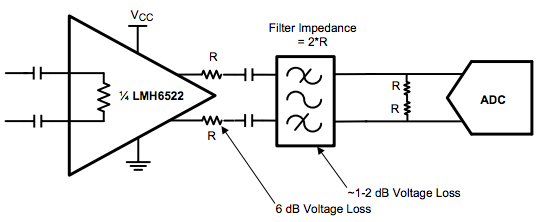
Filters are necessary to eliminate unwanted noise or distortion in a signal prior to any A/D conversion process. Designing a filter to pass the desired frequencies is easy, but it introduces signal loss, or insertion loss. Check out this application note from TI for some useful tips to optimize the filter design to minimize the losses.

Filter insertion losses
One of the first steps of filter optimization is the selection of the center frequency and the bandwidth of the filter. Once this step has been completed the task becomes one of putting the filter elements on the printed circuit board (PCB). PCB design is critical to filter performance, but even before we get to this stage we usually select both the component values and the component sizes we would like to use, this way we can allocate PCB space for the various components. As will be described later, it is very important to choose the filter components first, then make the necessary space available on the PCB, rather than trying to squeeze your filter into the space you have left at the end of the design. The components selected will be critical to the performance of your filter.
|
|