How to interface MAXIM’s DS1868 digital potentiometer with a PIC microcontroller
|
|
Potentiometers find applications in many electrical devices. For example, a light dimmer uses a potentiometer to control the brightness of lamps. In amplifiers, they are used to control the output volume of the music, or change the bass level. In an adjustable power supply we see potentiometers to vary the output voltage and current. In a frequency generator, they are used to control the duty cycle and frequency of the output signal. These potentiometers are electro-mechanical transducers that convert the rotary or linear displacement into a change in resistance. This change in resistance can be used to control anything from the brightness of a lamp to the direction of a rocket. But things have been changed lately. You can now vary the brightness of the lamp with touch switches. The volume of an amplifier can be controlled through a remote, and the frequency of an oscillator can be varied with tact switches. There are still potentiometers in these devices but in the form of silicon chips and not in the conventional electro-mechanical form. These are called digital potentiometers and today we will discuss about MAXIM’s DS1868 chip, which has two digitally controlled potentiometers. We will interface it to a PIC16F1827 microcontroller and vary the position of the wiper terminals from one end to the other.

Controlling the wiper position of DS1868 digital potentiometer
Theory
An analog potentiometer has three terminals, two of them are connected to the end-points of a resistive element of fixed resistance. The third terminal (known as wiper) can be slided to any point in between the two ends of the resistive element, thus varying the resistance between the wiper and any other end. A digital potentiometer mimics the same functionality except there are only finite wiper positions, which is is digitally controlled.

Pin diagram of DS1868 in 14-pin DIP

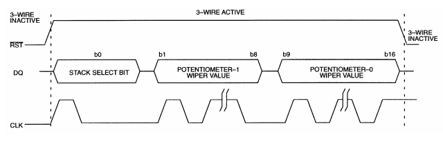
Timing diagram of signals over the 3-wire serial interface
For stack configuration and cascade operation, please refer the datasheet, they will not be covered here.
Circuit Diagram
I am going to use my PIC16F1827 development board for this experiment. The microcontroller runs at 16.0 MHz using external crystal or resonator. The high ends (H0 and H1) of the two digital potentiometers are connected to the supply voltage, whereas the low ends (L0 and L1) are grounded. The voltage at the wiper terminals thus varies from 0 to Vcc as their positions are slided from the lower end to the higher end. The two wiper terminal voltages are fed to two analog channels (AN0 and AN1) of the PIC16F1827. The RST, DQ, and CLK lines are driven through RA4, RB2, and RB3 port pins respectively. Two tact switches, ‘Up’ and ‘Down’, are connected to RA2 and RA3 pins. The microcontroller will read the key presses and slide the wiper terminals simultaneously towards appropriate direction based on what key is pressed. If the ‘Up’ key is pressed, the wiper will move one step towards the higher end. The size of the step can be set in the program for the PIC16F1827. The analog voltages from the wiper terminals are converted to 10-bit digital numbers using the on-board ADC module, and displayed on the LCD screen. Both the readings should match if the two potentiometers on the same DS1868 chip are identical. The microcontroller sends the display data to LCD in 4-bit mode through RB4-RB7 pins, whereas RS and E control pins are driven by RB0 and RB1 port pins.

Circuit diagram of the experiment

Circuit setup on the PIC16F1827 development board
Software
A driver routine for shifting in two 8-bit wiper positions and a stack selection bit to the 17-bit I/O register over the 3-wire serial interface is written in mikroC Pro for PIC compiler. Every time, Up/Down button is pressed, the potentiometer wiper positions are changed and the new AD conversion outputs are displayed on the LCD screen. Here’s the subroutine that transmits the 17-bit data over the 3-wire interface.
void Send_POT_Value(unsigned short num1){
 unsigned short t, Flag, Mask;
 Mask = 0x80;
 Reset = 1;    // Pull Reset line HIGH to initiate Data transfer
 Data = 0;     // Stack select bit 0
 Clock = 1;
 Delay_us(1);
 Clock = 0;

 // Shift in 8-bit wiper position for POT1
 for (t=0; t<8; t++){
   Flag = num1 & Mask;
   if(Flag==0) Data = 0;
   else Data = 1;
   Clock = 1;
   Delay_us(1);
   Clock = 0;
   Mask = Mask >> 1;
 }
 // Shift in 8-bit wiper position for POT0
 Mask = 0x80;
 for (t=0; t<8; t++){
  Flag = num1 & Mask;
  if(Flag==0) Data = 0;
  else Data = 1;
  Clock = 1;
  Delay_us(1);
  Clock = 0;
  Mask = Mask >> 1;
 }
 Reset = 0;   // End Data transfer
}
Output
By pressing the Up and Down buttons you can vary the wiper positions of the two potentiometer which is displayed on LCD screen as 10-bit digital values (varying between 0 to 1023).

Varying the wiper position varies the voltage divider output, and so the AD conversion values
The two potentiometer inside the DS1868 chip are found consistent within ±1 count of 10-bit AD conversion result. When the wiper positions are set to 255, they should reach the higher ends, H0 and H1, of the potentiometers. But it seems like they are little bit off from that because the AD conversion result for those wiper positions went only up to 1019 (4 counts less than the AD saturation value, 1023), which is actually off by 0.04K? (not significant) for a 10K? DS1868 potentiometer.
|
|
In proteus software which file should be given as input i mean ex.wav,mp3 etc
Hello.. can any easy used of microcontroller for control the gain from amplifier as automatically. based from signal or power input.???
Pingback: Blog J.Schweiss | AVR Tutorials
Sout and Cout are for stacked and cascade configurations and are not used here.
where to connect Sout and Cout pins???
I think the shift at the upper end is caused by the Wiper resistance. According to the DS1868 datasheet the wiper resistence is typically 400 Ohms (max 1000 Ohms).
I don’t know how you measured/calculated it as 40 Ohms thou…
Best wishes
Bülent Özden
Pingback: Electronics-Lab.com Blog » Blog Archive » Using DS1868 digital potentiometer with PIC microcontroller
Thanx yar