Understanding Logic Analyzer basics using SCANALOGIC-2 EDU KIT
|
|
A logic analyzer is an excellent tool for capturing many digital signals at once and displaying their timing relationships. It is particularly useful in verifying and debugging digital circuits. This tutorial is intended to provide a quick overview of a logic analyzer tool and its uses in analyzing and decoding data flowing on multiple signal lines or bus in a digital system. The logic analyzer tool is extremely helpful in troubleshooting problems arising from timing violations and transients on buses. In this article, I am going to use the SCANALOGIC-2 educational kit from IKALOGIC to illustrate very basic features of a logic analyzer.
Logic analyzer vs oscilloscope
Several types of electronic measurement tools are used to test and verify digital circuits. A digital oscilloscope is one of the most commonly used tools in an electronics lab. The oscilloscope is used for general-purpose signal viewing and it allows to make accurate measurements of various attributes of the signal such as rise- and fall-times, peak amplitude, frequency, the elapsed time between edges, etc. Typical digital oscilloscopes have up to four signal inputs, which means you can simultaneously observe four signals and their attributes. However, the oscilloscope cannot help you when you need to measure digital signals on a 32-bit microcprocessor bus simultaneously because it doesn’t have that many channels. A logic analyzer tool can serve this purpose. Although it grew out of an oscilloscope, the logic analyzer have different capabilities, and it measures and analyzes signals differently than an oscilloscope. Instead of measuring analog details, the logic analyzer only detects the logic state of a signal. Logic analyzers can have over 100 channels (some sophisticated ones have over thousand channels). Because they can capture and display logic states of many signal lines at once, logic analyzers are very helpful for verifying time relationship between the signals. They can also decode information sent over the microprocessor bus and present them in a meaningful form.
Logic analyzers present data basically in the same way as oscilloscopes do with time axis along horizontal. But the vertical axis of logic analyzer has only 1-bit resolution required to indicate either a logic High or a logic Low. When you connect a logic analyzer to a digital circuit, you’re only concerned with the logic state of the signal, and not analog details as oscilloscopes do. Besides, logic analyzers can’t display data in real time. They first capture the signals and display them later. They are very useful when looking at time relationship between many signals at one glance. It can also decode information sent over the microprocessor buses and present them in a meaningful form.
The basic defining characteristics of a logic analyzer are the number of input channels it can sample, the maximum sampling rate, and the memory depth for storing the samples. The specification of memory depth defines how many captured samples can be stored per channel in a single run. For example, an analyzer with 32K depth can store 32K samples per channel. If you use a sampling frequency of 1 million samples per second, then it will fill up just in 32 milliseconds. Larger memory depths allow you to sample data for longer time, which is helpful to spot and correct a timing violation on bus.
Modes
Logic analyzers have two basic modes of operation: timing mode and state mode.
In timing mode, the data is sampled at regular intervals according to a clock internal to the logic analyzer. As such there is no fixed timing relationship between a target system and the samples acquired by the logic analyzer. The samples are stored in the memory and are used later to analyze the timing relationship between the signals. This mode of operation is also known as asynchronous acquisition and is useful in debugging mostly hardware problems.
The timing relationship between the signals is not particularly useful while tracking down software related problems. The software developer is more interested to see the instruction flow of the program. In state mode, a signal from the target device (usually a microprocessor clock) defines the sample point. Signals are captured on the active edge of every clock signal received from the target device. In this case, the relative timing information between the signals is unimportant. Since the data are sampled during the active edge of the system clock, the logic signals are stable and represent a valid state of the target system. Therefore, with multiple samples, it is possible to capture and display successive states of the system in a sequence. This points up the major difference between timing and state mode. The timing analyzer has an internal clock to control sampling, so it asynchronously samples the system under test. A state analyzer synchronously samples the system since it gets its sampling clock from the system.
Triggering
A logic analyzer needs a trigger signal that basically tells it when to start recording samples. Since a logic analyzer has a limited amount of memory for storing samples, a trigger helps to capture the action of interest properly. A trigger is normally defined by a logic condition built on the sampled data that has to be met in order to capture the data. Many conditions can be used to trigger a logic analyzer. For example, a change in the logic state of a single line can be used as a trigger. Similarly, in a more complex system, recognizing a specific binary value on a bus or a sequence of pre-defined data values can be used as triggers. Although there is no theoretical limit on how you would define a trigger, complex trigger algorithms are difficult to implement because the trigger event has to be evaluated in real time.
SCANALOGIC-2
SCANALOGIC-2 is an educational kit that allows you to build a low-cost four channel logic analyzer at home. It is based on ATMEL’s Atmega168 microcontroller. It connects to a PC through USB port and uses a free PC software called ScanaStudio to visualize and analyze the captured signals. The key features of SCANALOGIC-2 are:
- Sampling rate: 20 Million samples per seconds
- No. of channels: 4
- Memory depth: 256K per channel (total 1 MByte)
- Protocol decoding: I2C, SPI, UART, 1-Wire
- Digital output capability: PWM, FM, UART packets
When you order the Scanalogic-2 EDU KIT, the board comes with presoldered SMT components that include the microcontroller, memory chips, I/O buffer chips and quartz oscillator. Rest of the through-hole components (resistors, capacitors, regulator IC, and diodes) are to be soldered by yourself, which is pretty easy. The KIT also includes gripper probes to hook the logic analyzer to your circuit.
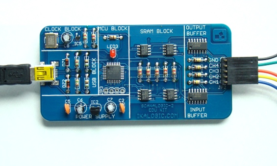
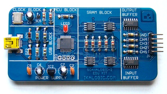
The picture below shows an assembled SCANALOGIC-2 board. It consists of six distinct blocks, marked by top silkscreen, that describes how a typical logic analyzer works.
- Power Supply Block provides stable and filtered 3.6V for the memory and I/O buffer chips.
- USB Block allows the voltage matching between the USB signal levels (3.3V) and the microcontroller’s 5V logic outputs.
- Clock Block provides a stable 20MHz clock for the operation of the microcontroller and for the signal sampling.
- MCU Block contains the Atmega168 microcontroller, which is the heart of the device. It received the capture request from the host (PC) application, initializes the SRAM ICs, watches for trigger conditions and records the exact trigger position. It sends the captured samples to the host application for further analysis and visualization.
- SRAM Block holds the sampled data. There are 4 SRAMs, one for each channel. Each byte of data represents 8 consecutive samples, one for each bit. The logic samples are directly fed into the SRAMs, bypassing through the microcontroller, to achieve the maximum sampling frequency of 20 MHz.
- BUFFER Block isolates the outside world from the logic analyzer. Besides, it also helps to interface a variety of logic levels from 2.0-5.0V.
Test Setup
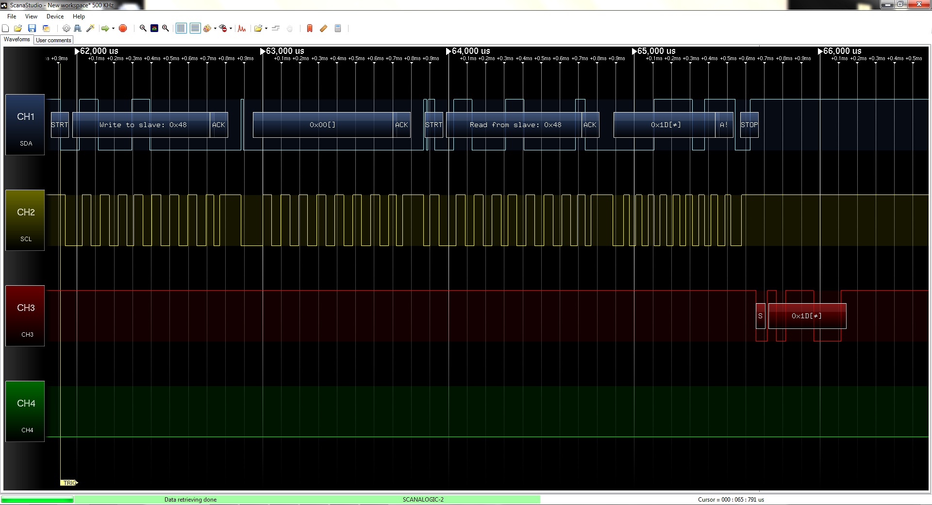
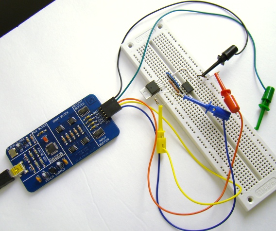
Now we will setup a very simple test circuit to see SCANALOGIC-2 in action. The test setup consists of the PIC12F683 microcontroller and TC74 temperature sensor. The communication with the TC74 device is accomplished via a 2-wire I2C compatible serial bus. The PIC12F683 microcontroller is programmed to access the temperature reading from the TC74 device using I2C bus and send it out to its UART TX port. Channels 1 through 3 of SCANALOGIC-2 are connected to the I2C-SDA, I2C-SCL, and UART-TX signal lines, respectively, to monitor the data flow on these lines. The logic analyzer is connected to a PC that has the ScanaStudio software installed to visualize the captured data. Note that the SCANALOGIC-2 analyzer works in timing mode only.
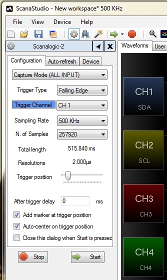
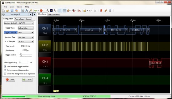
Scanastudio also allows to select Trigger Channel and Trigger Type before you capture data. In this case, I have setup Channel 1 as ‘Trigger Channel’, with ‘Trigger Type’ to be a Falling Edge, which means data capturing will start when a high-to-low falling pulse is detected on the I2C-SDA line, which could happen during an I2C Start signal. The sampling rate for the test case has been selected to be 500KHz , which is good enough to analyze the I2C communication (happening at 100 KHz) between PIC12F683 and TC74.
The following picture is a Scanastudio snapshot visualizing the captured data on Channels 1 through 3. It is much easier to analyze the captured data if protocol decoder is enabled. Scanastudio software can decode I2C, SPI, UART, and 1-Wire protocols. Read SCANALOGIC-2 manual for more detail on this. I have setup I2C protocol decoder (with 7-bit slave address, and R/W) on CH1 and CH2, and UART decoder on CH3.
Reading temperature from the TC74 device through I2C port involves the following steps:
- The host microcontroller issues a Start condition followed by the address byte. The address byte consists of the 7-bit slave address (0x48) and a Read/Write bit (R/W). The R/W bit is always ’0? (Write) in the first phase.
- If the received 7-bit address matches with its own address, the TC74 device responds with an acknowledge pulse.
- The host microcontroller next sends the command byte to TC74 to indicate which register it wants to access. For reading the temperature, the command byte should be 00h. The TC74 responds with an acknowledge pulse.
- The host microcontroller issues a new Start condition because the direction of data transfer is now going to be changed. The new address byte with R/W bit 1 is sent by the host, which is acknowledged by the slave.
- The TC74 transmits the 8-bit temperature data (°C) from the temperature register. Upon receiving the byte, the host doesn’t acknowledge, but generates a Stop condition.
In the following pictures (screenshots of Scanastudio running on PC), you can see how the logic analyzer captures all these events happening on the I2C bus while the PIC12F683 microcontroller reads temperature from the TC74 device.
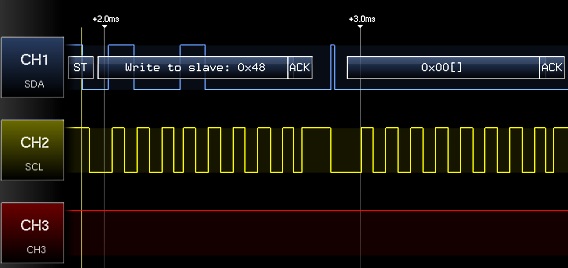
PIC12F683 initiates communication with Start signal and then sends a 7-bit slave address (0x48) followed by a R/W bit 0 (Write). TC74 responds with an acknowledge pulse. Next, PIC12F683 sends temperature read command (0x00), which is also acknowledged by TC74.
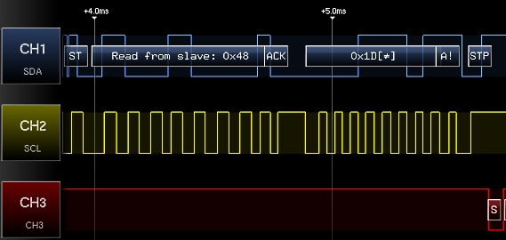
PIC12F683 issues a new Start condition with R/W bit set to 1 (Read). This is acknowledged by TC74. PIC12F683 receives a temperature byte from TC74, and sends a STOP signal without sending any acknowledgement pulse. The received byte is 0x1D (29 decimal) which corresponds to 29 °C.
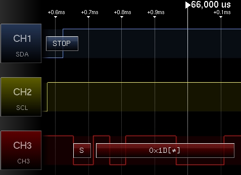
PIC12F683 sends out the received temperature byte (0x1D) on UART-TX line, which is hooked up to CH3 of SCANALOGIC-2.
Summary
A brief overview of logic analyzer was presented in this tutorial along with a quick review of Ikalogic’s SCANALOGIC-2 EDU kit that allows you to build a simple and low-cost 4-channel logic analyzer at home. The SCANALOGIC-2 is based on ATMEL’s Atmega168 microcontroller and provides 20MHz sampling rate with 256K memory depth per channel. It uses the Scanastudio software on PC for visualizing the captured data. The software supports I2C, SPI, UART, and 1-wire protocol decoding on its four channels. The SCANALOGIC-2 channels also have got digital output capabilities that were not discussed here. You can refer the product manual to find more details on that.
To sum up, SCANALOGIC-2 is a very simple and inexpensive logic analyzer kit that can come in very useful for beginners and hobbyists to analyze and debug serial interfaces between microcontroller and peripherals. It can also be used to generate PWM, Frequency Modulation, and UART signals for testing purpose. There is a plenty of room for further improvements too. IkaLogic should consider expanding the number of input channels, increasing memory depth, and implementing more trigger options.
References
1. The XYZs of Logic Analyzers from Textronix
|
|

The basic defining characteristics of a logic analyzer are the number of input channels it can sample, the maximum sampling rate, and the memory depth for storing the samples.
Pingback: Understanding Logic Analyzer basics using SCANALOGIC-2 EDU KIT -Use Arduino for Projects
Pingback: Blog J.Schweiss | LogAnalyzer