XMega DAC
|
|
In embedded systems, oftentimes it is needed to generate analog outputs from a microcontroller. Examples of such include, generating audio tones, voice, music, smooth continuous waveforms, function generators, voltage reference generators, etc. Traditionally in such cases the most common techniques applied are based on Pulse Width Modulation (PWM), resistor networks and external Digital-to-Analog Converter (DAC) chips like MCP4921. The aforementioned techniques have different individual limitations and moreover require external hardware interfacing, adding complexities and extra cost to projects. XMega micros are equipped with 12 bit fast DACs apart from PWM blocks and again it proves itself to be a very versatile family of microcontrollers. In this post we will have a look into this block.
A brief overview
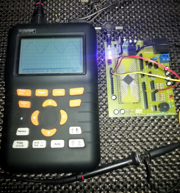
I used ATXMega32A4U just as always and it has only one dual channel DAC designated DACB but there are other XMega devices that have more than one DAC.
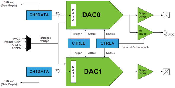
The internal block diagram of the DAC block above shows its major parts. The DAC of XMega is perhaps one of the simplest block to understand. Apart from DMA and event system interfacing, the DAC can provide reference source for the analog comparator and ADC blocks. It also has the capability to directly drive both resistive and capacitive loads (check device datasheet for limits). Just like the ADC block, the DAC block itself needs a reference source and this reference source can be both internal (internal 1.0V reference) and external (AVCC or AVREF). As stated earlier there are two independent DAC channels in the XMega32A4U and so there are two separate analog outputs (PB2 and PB3) available from this micro.
The basic formula for voltage output from the DAC is as follows:
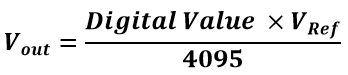
The digital data value ranges from 0 – 4095 (0x0000 – 0x0FFF) since it is a 12 bit DAC. How fast it can operate will depend on peripheral clock’s operating frequency. Just like the clock system, the DAC output can be precisely calibrated by using gain error and offset error registers. Though calibrating the DAC ensures more accurate data output, it is seldom used. If it is needed to calibrate the DAC for sensitive operations one must do so carefully and should use standard instruments that have least possible error, otherwise it is pointless to calibrate it. You can use the XMega ADC block for calibration purpose if you don’t have access to good measurement instruments. In my previous post I showed how to use the XMega ADC. I, however, never calibrated the DAC block. Calibration process is well explained in the reference manual.
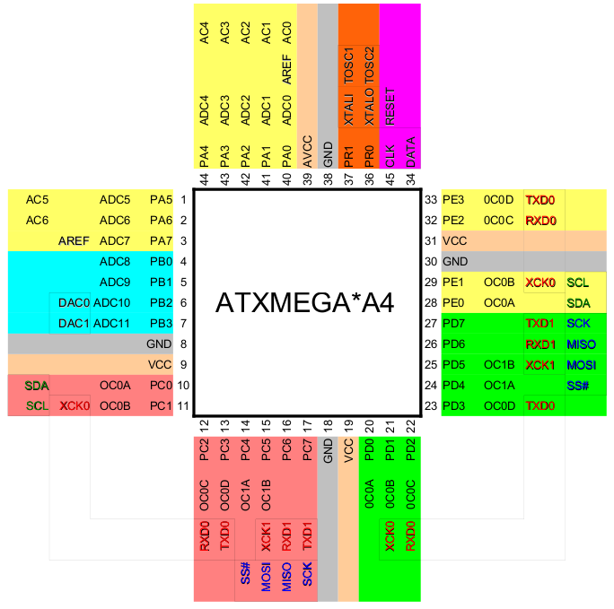
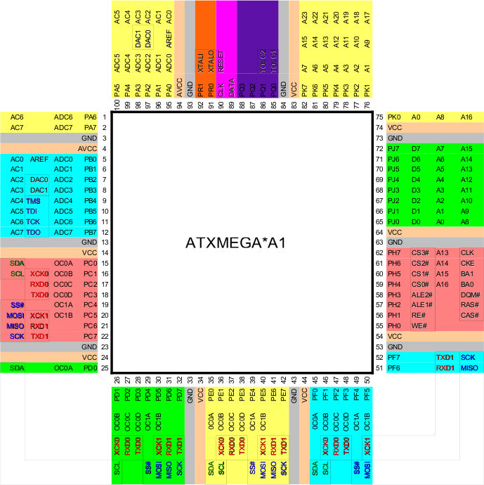
Shown below are pin diagrams of both the most popular XMega A1 and A4 devices. Checkout the DAC output pin locations because these are not mentioned in the reference manual.
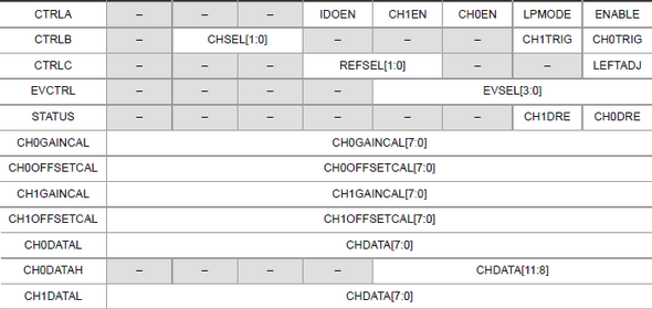
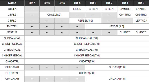
Registers
The simplified register map for the DAC block shows that there are only a few registers to deal with. I’m not going to detail about them as the reference manuals are already doing so.
Control registers A-C are sequentially set first. These registers are responsible for selecting reference source, channel, power mode, etc. Calibration registers have names ending with “CAL” and data input registers have names ending with “DATA”. Lastly there is event system register that select which event system channel would trigger the DAC and there is a STATUS register which flags when it is possible to write new values to a specific DAC channel.
Coding
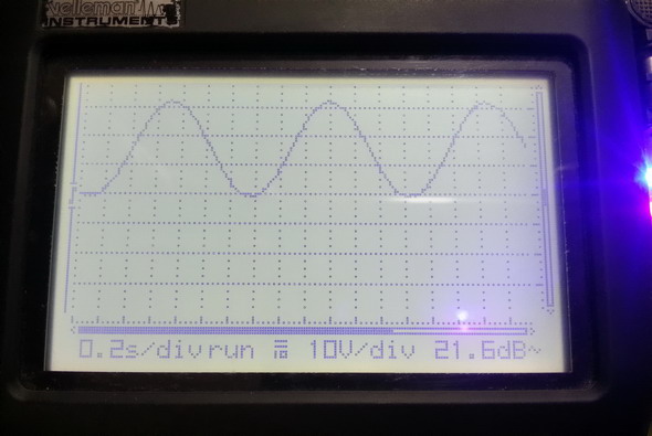
The code, just as in previous posts, starts with clock and I/O configuration setups and then the DAC is setup. In this code example I coded the XMega as such that both of its outputs will give sinusoidal voltage variations or in other words the DAC output pins will output sine wave signals. I also coded a DAC header file for quick coding and less meddling with register values. The DAC block is coded to use (3.3V) as reference source and both DAC channels are employed. One DAC channel will output sine wave output while the other at the same instance will give out phase shifted sine wave or cosine wave signal. MikroC CMath library is used for the trigonometric (sine-cosine) functions. PB2 and PB3 are set as output pins. Lastly left adjustment of DAC data is avoided to keep things simple. Please note that I didn’t calibrate the DAC and still it worked good enough.
#include "clock.h"
#include "dac.h"
#include "io.h"
void setup();
void clock_setup();
void io_setup();
void dac_Setup();
void dac_write(unsigned char channel, unsigned int value);
void main()
{
signed int temp1 = 0;
signed int temp2 = 0;
unsigned int degree = 0;
setup();
while(1)
{
for(degree = 0; degree < 360; degree++)
{
temp1 = (2047 * cos(degree * 0.0174532925));
temp1 = (2048 - temp1);
temp2 = (2047 * sin(degree * 0.0174532925));
temp2 = (2048 - temp2);
dac_write(0, ((unsigned int)temp1));
dac_write(1, ((unsigned int)temp2));
delay_us(10);
}
};
}
void setup()
{
clock_setup();
io_setup();
dac_Setup();
}
void clock_setup()
{
OSC_CTRL |= OSC_RC32KEN_bm;
while(!(OSC_STATUS & OSC_RC32KRDY_bm));
OSC_CTRL |= OSC_RC32MEN_bm;
CPU_CCP = CCP_IOREG_gc;
CLK_PSCTRL = ((CLK_PSCTRL & (~(CLK_PSADIV_gm | CLK_PSBCDIV1_bm
| CLK_PSBCDIV0_bm))) | CLK_PSADIV_1_gc | CLK_PSBCDIV_2_2_gc);
OSC_DFLLCTRL = ((OSC_DFLLCTRL & (~(OSC_RC32MCREF_gm | OSC_RC2MCREF_bm))) |
OSC_RC32MCREF_RC32K_gc);
DFLLRC32M_CTRL |= DFLL_ENABLE_bm;
while(!(OSC_STATUS & OSC_RC32MRDY_bm));
CPU_CCP = CCP_IOREG_gc;
CLK_CTRL = ((CLK_CTRL & (~CLK_SCLKSEL_gm)) | CLK_SCLKSEL_RC32M_gc);
OSC_CTRL &= (~(OSC_RC2MEN_bm | OSC_XOSCEN_bm | OSC_PLLEN_bm));
PORTCFG_CLKEVOUT = 0x00;
}
void io_setup()
{
PORTB_OUT = 0x00;
PORTB_DIR = 0x0C;
PORTB_PIN0CTRL = (PORT_OPC_TOTEM_gc | PORT_ISC_BOTHEDGES_gc);
PORTB_PIN1CTRL = (PORT_OPC_TOTEM_gc | PORT_ISC_BOTHEDGES_gc);
PORTB_PIN2CTRL = (PORT_OPC_TOTEM_gc | PORT_ISC_INPUT_DISABLE_gc);
PORTB_PIN3CTRL = (PORT_OPC_TOTEM_gc | PORT_ISC_INPUT_DISABLE_gc);
PORTB_INT0MASK = 0x00;
PORTB_INT1MASK = 0x00;
}
void dac_setup()
{
DACB_CTRLA = ((DACB_CTRLA & (~(DAC_IDOEN_bm | DAC_CH0EN_bm | DAC_CH1EN_bm
| DAC_LPMODE_bm))) | DAC_CH0EN_bm | DAC_CH1EN_bm | DAC_ENABLE_bm);
DACB_CTRLB = ((DACB_CTRLB & (~(DAC_CHSEL_gm | DAC_CH0TRIG_bm
| DAC_CH1TRIG_bm))) | DAC_CHSEL_DUAL_gc);
DACB_CTRLC = ((DACB_CTRLC & (~(DAC_REFSEL_gm | DAC_LEFTADJ_bm)))
| DAC_REFSEL_AVCC_gc);
}
void dac_write(unsigned char channel, unsigned int value)
{
switch(channel)
{
case 0:
{
while(!(DACB_STATUS & DAC_CH0DRE_bm));
DACB_CH0DATA = value;
break;
}
case 1:
{
while(!(DACB_STATUS & DAC_CH1DRE_bm));
DACB_CH1DATA = value;
break;
}
}
}
XMega DAC Demo
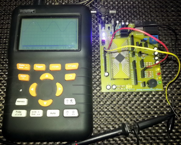
Demo video link: https://www.youtube.com/watch?v=O61v0nww6vU.
Files: XMega DAC
References: XMega AU Manual and Datasheet.
Happy coding.
Author: Shawon M. Shahryiar https://www.facebook.com/groups/microarena/ https://www.facebook.com/MicroArena +8801970046495 26.01.2015|
|
Pingback: XMega DAC -Use Arduino for Projects