Tinkering TI MSP430F5529
|
|
ADC12 Interrupt
ADC interrupt is as important as timer and communication interrupts. We can do other tasks while ADC is performing a conversion.
Code Example
#include "driverlib.h"
#include "delay.h"
#include "lcd.h"
#include "lcd_print.h"

unsigned long cnt = 0;

void clock_init(void);
void GPIO_init(void);
void ADC12_init(void);

#pragma vector = ADC12_VECTOR
__interrupt void ADC12ISR (void)
{
    switch (__even_in_range(ADC12IV, 34))
    {
        case  0: break;   //Vector  0:  No interrupt
        case  2: break;   //Vector  2:  ADC overflow
        case  4: break;   //Vector  4:  ADC timing overflow
        case  6:          //Vector  6:  ADC12IFG0
        {
            cnt = ADC12_A_getResults(ADC12_A_BASE,
                                     ADC12_A_MEMORY_0);
            break;
        }
        case  8: break;   //Vector  8:  ADC12IFG1
        case 10: break;   //Vector 10:  ADC12IFG2
        case 12: break;   //Vector 12:  ADC12IFG3
        case 14: break;   //Vector 14:  ADC12IFG4
        case 16: break;   //Vector 16:  ADC12IFG5
        case 18: break;   //Vector 18:  ADC12IFG6
        case 20: break;   //Vector 20:  ADC12IFG7
        case 22: break;   //Vector 22:  ADC12IFG8
        case 24: break;   //Vector 24:  ADC12IFG9
        case 26: break;   //Vector 26:  ADC12IFG10
        case 28: break;   //Vector 28:  ADC12IFG11
        case 30: break;   //Vector 30:  ADC12IFG12
        case 32: break;   //Vector 32:  ADC12IFG13
        case 34: break;   //Vector 34:  ADC12IFG14
        default: break;
    }
}

void main(void)
{
    unsigned long volts = 0;

    WDT_A_hold(WDT_A_BASE);

    clock_init();
    GPIO_init();
    ADC12_init();

    LCD_init();
    LCD_clear_home();

    LCD_goto(0, 0);
    LCD_putstr("ADC Count:");

    LCD_goto(0, 1);
    LCD_putstr("Volts/mV :");

    while(1)
    {
        volts = ((cnt * 3300) / 4095);
        print_I(11, 0, cnt);
        print_I(11, 1, volts);
        delay_ms(100);
    };
}

void clock_init(void)
{
    PMM_setVCore(PMM_CORE_LEVEL_3);

    GPIO_setAsPeripheralModuleFunctionInputPin(GPIO_PORT_P5,
                                               (GPIO_PIN4 | GPIO_PIN2));

    GPIO_setAsPeripheralModuleFunctionOutputPin(GPIO_PORT_P5,
                                                (GPIO_PIN5 | GPIO_PIN3));

    UCS_setExternalClockSource(XT1_FREQ,
                               XT2_FREQ);

    UCS_turnOnXT2(UCS_XT2_DRIVE_4MHZ_8MHZ);

    UCS_turnOnLFXT1(UCS_XT1_DRIVE_0,
                    UCS_XCAP_3);

    UCS_initClockSignal(UCS_FLLREF,
                        UCS_XT2CLK_SELECT,
                        UCS_CLOCK_DIVIDER_4);

    UCS_initFLLSettle(MCLK_KHZ,
                      MCLK_FLLREF_RATIO);

    UCS_initClockSignal(UCS_SMCLK,
                        UCS_XT2CLK_SELECT,
                        UCS_CLOCK_DIVIDER_2);

    UCS_initClockSignal(UCS_ACLK,
                        UCS_XT1CLK_SELECT,
                        UCS_CLOCK_DIVIDER_1);
}

void GPIO_init(void)
{
    GPIO_setAsOutputPin(GPIO_PORT_P4,
                        GPIO_PIN7);

    GPIO_setAsPeripheralModuleFunctionInputPin(GPIO_PORT_P6,
                                               GPIO_PIN0);
}


void ADC12_init(void)
{
    ADC12_A_configureMemoryParam configureMemoryParam = {0};

    ADC12_A_init(ADC12_A_BASE,
                 ADC12_A_SAMPLEHOLDSOURCE_SC,
                 ADC12_A_CLOCKSOURCE_ACLK,
                 ADC12_A_CLOCKDIVIDER_1);

    ADC12_A_setupSamplingTimer(ADC12_A_BASE,
                               ADC12_A_CYCLEHOLD_768_CYCLES,
                               ADC12_A_CYCLEHOLD_4_CYCLES,
                               ADC12_A_MULTIPLESAMPLESENABLE);

    ADC12_A_setResolution(ADC12_A_BASE,
                          ADC12_A_RESOLUTION_12BIT);

    configureMemoryParam.memoryBufferControlIndex = ADC12_A_MEMORY_0;
    configureMemoryParam.inputSourceSelect = ADC12_A_INPUT_A0;
    configureMemoryParam.positiveRefVoltageSourceSelect = ADC12_A_VREFPOS_AVCC;
    configureMemoryParam.negativeRefVoltageSourceSelect = ADC12_A_VREFNEG_AVSS;
    configureMemoryParam.endOfSequence = ADC12_A_NOTENDOFSEQUENCE;

    ADC12_A_configureMemory(ADC12_A_BASE,
                            &configureMemoryParam);

    ADC12_A_clearInterrupt(ADC12_A_BASE,
                           ADC12IFG0);

    ADC12_A_enableInterrupt(ADC12_A_BASE,
                            ADC12IE0);

    __enable_interrupt();

    ADC12_A_enable(ADC12_A_BASE);

    ADC12_A_startConversion(ADC12_A_BASE,
                            ADC12_A_MEMORY_0,
                            ADC12_A_REPEATED_SINGLECHANNEL);
}
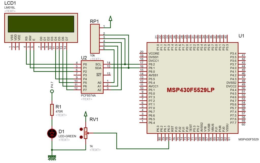
Hardware Setup
Explanation
This example is similar to the last one in many aspects. I won’t be going through all settings. I’ll only highlight the key differences.
This time an external ADC channel is used and so we have to initialize the alternative role of its pin.
GPIO_setAsPeripheralModuleFunctionInputPin(GPIO_PORT_P6, GPIO_PIN0);
In the ADC12 initialization, the external input pin or the ADC channel’s physical pin is set after its GPIO initialization. Unlike the last ADC example in which we used internal 1.5V reference source, the positive reference source for ADC this time is set to AVCC. AVSS is the negative voltage source for both examples. AVCC is same as the system bus voltage, i.e. 3.3V.
configureMemoryParam.inputSourceSelect = ADC12_A_INPUT_A0;
configureMemoryParam.positiveRefVoltageSourceSelect = ADC12_A_VREFPOS_AVCC;
configureMemoryParam.negativeRefVoltageSourceSelect = ADC12_A_VREFNEG_AVSS;
Since we are using interrupt method, relevant interrupt flag is cleared first and then enabled.
ADC12_A_clearInterrupt(ADC12_A_BASE, ADC12IFG0);
ADC12_A_enableInterrupt(ADC12_A_BASE, ADC12IE0);
__enable_interrupt();
In this case the 0th ADC interrupt flag is used since the channel to be read is the 0th channel of the ADC. Don’t confuse interrupt vector number with interrupt flag number. Interrupt vector number for 0th ADC interrupt flag is 6.
#pragma vector = ADC12_VECTOR
__interrupt void ADC12ISR (void)
{
    switch (__even_in_range(ADC12IV, 34))
    {
        case  0: break;   //Vector  0:  No interrupt
        case  2: break;   //Vector  2:  ADC overflow
        case  4: break;   //Vector  4:  ADC timing overflow
        case  6:          //Vector  6:  ADC12IFG0
        {
            cnt = ADC12_A_getResults(ADC12_A_BASE,
                                     ADC12_A_MEMORY_0);
            break;
        }
        case  8: break;   //Vector  8:  ADC12IFG1
        case 10: break;   //Vector 10:  ADC12IFG2
        case 12: break;   //Vector 12:  ADC12IFG3
        case 14: break;   //Vector 14:  ADC12IFG4
        case 16: break;   //Vector 16:  ADC12IFG5
        case 18: break;   //Vector 18:  ADC12IFG6
        case 20: break;   //Vector 20:  ADC12IFG7
        case 22: break;   //Vector 22:  ADC12IFG8
        case 24: break;   //Vector 24:  ADC12IFG9
        case 26: break;   //Vector 26:  ADC12IFG10
        case 28: break;   //Vector 28:  ADC12IFG11
        case 30: break;   //Vector 30:  ADC12IFG12
        case 32: break;   //Vector 32:  ADC12IFG13
        case 34: break;   //Vector 34:  ADC12IFG14
        default: break;
    }
}
ADC interrupt triggers when a new result is loaded in ADC memory location. Inside the interrupt ADC memory location 0 is read to get the conversion result, i.e. ADC count. When the ADC memory is accessed, its interrupt flag is automatically cleared.
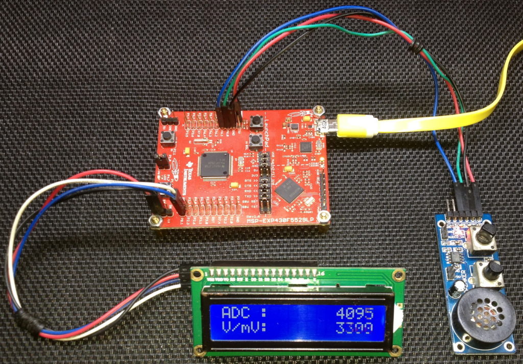
In the main loop, the ADC count derived from the ADC interrupt is converted to voltage. Both the voltage and ADC count are displayed on an alphanumerical LCD.
volts = ((cnt * 3300) / 4095);
print_I(11, 0, cnt);
print_I(11, 1, volts);
delay_ms(100);
Demo
|
|
Hello, dear sir Shawon Shahryiar, could you send me the GRACE program by email? I can’t find it anywhere on the Internet. Thank you very much and all the best.
https://www.dropbox.com/scl/fi/6jgmxuuwl9dw2zo9mpuwm/grace_setup_2.2.0.00006.rar?rlkey=gm20hy3odiuyajjow2pas3iz0&st=hhfakdjt&dl=0
Hello, what software are you using for the Hardware setup images and does it support simulation for the MSP430F5529
I used Proteus VSM for drawing schematics but it doesn’t support simulation.
Hi,
Im interfacing MSP430F5529 with MAX17055 fuel guage. while reading 16 bit value, the first byte im receiving is 0. so while reading multiple registers continuously the data exchange is happening, but im getting the correct data. Can anyone suggest me what will be the issue? why im getting 0 in first byte?
read16_bit data code:
uint16_t value = 0;
USCI_B_I2C_setslaveaddress(USCI_B1_BASE, slave_address);
USCI_B_I2C_setmode(USCI_B1_BASE, USCI_B_I2C_TRANSMIT_MODE);
USCI_B_I2C_masterSendStart(USCI_B1_BASE);
while (!USCI_B_I2C_masterSendStart(USCI_B1_BASE));
USCI_B_I2C_mastterSendSingleByte(USCI_B1_BASE, reg_address);
USCI_B_I2C_setslaveaddress(USCI_B1_BASE, slave_address);
USCI_B_I2C_setmode(USCI_B1_BASE, USCI_B_I2C_TRANSMIT_MODE);
USCI_B_I2C_masterReceiveMultiByteStart(USCI_B1_BASE);
uint8_t lb = USCI_B_I2C_masterReceiveMultiByteNext(USCI_B1_BASE);
uint8_t hb = USCI_B_I2C_masterReceiveMultiByteFinish(USCI_B1_BASE);
while (USCI_B_I2C_isBusBusy(USCI_B_BASE));
value = lb << 8;
value |= hb;
return value;
In code, after sending reg address, it will be recieve mode. its a type mistake
Hi, im trying to send the command from the terminal view. i can able to send the command and tried to blink p1.0 led in msp430f5529 controller, its working fine. And im using led driver IS31FL3236A interfaced with msp430f5529 controller, i can able to interface im getting the expected output.
now i need to send the command from seriak monitor based on that command i2c communication need to start. both communication are working fine, when it runs separately. its not working when i tried to combine.
any one had any idea, why it is happening or what will be the issue?
It could be due to:
1. conflicts in clock settings
2. hardware conflict like pin mapping
3. code is getting stuck or waiting for one communication line to finish
4. use of polling method instead of interrupt-driven coding
Hi, thank you for the respose.
Do I need to use different clock initialization for I2C and UART communication? if YES, can you explain how to do that?
I mean check which clock has been set for UART and I2C…. Is it SMCLK, MCLK, etc and is it tuned to right frequency required by the respective hardware?
Is there any example on how to implement polling method in uart?
Why go for polling method when it is a blocking method of coding? It is better to use interrupts instead at least for UART receive.
yes!! currently in my code, only for uart im using interrupts to recieve command from serial monitor. Im not using interrupt for I2C communication.
so the issue is must be in clock initialization. right?
For UART, im using USCI_A1_BASE. and for I2C, im using USCI_B1_BASE.
And another thing i need to ask is, in uart when i tried blink led(p1.0) in msp430f5529 by passing command. here, without clock I’m getting output. how it is possible?
And for both i2c and uart i gave SMCLK with 1Mhz
I am surprised and happy to find this tutorial on the F5529 as TI makes a lot of different devices.
Thank you very much for putting in the extra knowledge in each segment, made reading worthwhile.
Good Work!
lovely tutorial but to be honest I don’t think I’d be investing my time on this board to start with it’s not cheap and readily available as the stm32 boards can you please do more tutorials on stm32 board’s and the stc micros thanks
Hello, I try to program MSP430FR6047 but i get error “the debug interface to the device has been secured”. when flashing using uniflash and when program using CCS this happen. can you help me to solve this problem
You can try “On connect, erase user code and unlock the device” option.
Pingback: Tinkering TI MSP430F5529 – gStore
Hello
I am doing project of msp430g2553 interface(using i2c communication) with temp 100(temperature sensor) and try to read the temperature in dispaly(16*2) but didn’t get the out put (using code composer studio) can u share me any example code for this project
Thank you sir,
Which sensor? Did you use pullup resistors for SDA-SCL pins?
Where is lcd_print.h?
All files and docs are here:
https://libstock.mikroe.com/projects/view/3233/tinkering-ti-msp430f5529
You want the truth? TI makes and sell “underpowered micros”, you know? Low everything, not only the power but also peripherals. So the price is not justified.
Otherwise, if I’ll move there, I’ll introduce them to my small hobby projects – there are still some advantages.
I may even make a visual configuration tool of my own for them…
Yeah the prices of TI products are higher than other manufacturers but I don’t think the hardware peripherals are inferior.
Not inferior but in not enough numbers compared to STM32.
True