Tinkering TI MSP430F5529
|
|
ADC12 and Direct Memory Access (DMA) Module
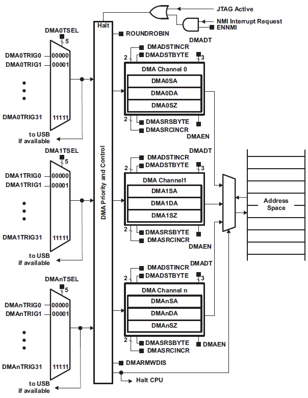
Apart from interrupt method, there is another way to doing AD conversions without polling/waiting. This involves DMA-backed AD conversion. DMA hardware is not a part of the ADC. In simple terms, it is rather more like a separate data pipeline bus that can be used without much interaction from the CPU. DMA-based AD conversions are in that way very silent. DMA can send AD conversion readings directly to user-defined memory locations automatically without any intervention. DMA can also be used for other hardware like SPI and UART. Shown below is the DMA block diagram of MSP430F5529:
Code Example
#include "driverlib.h"
#include "delay.h"
#include "lcd.h"
#include "lcd_print.h"

void clock_init(void);
void GPIO_init(void);
void ADC12_init(void);
void DMA_HW_init(void);

uint16_t memory_location = 0x0000;

#pragma vector = DMA_VECTOR
__interrupt void DMA_ISR (void)
{
    switch (__even_in_range(DMAIV, 16))
    {
        case 0: break;  //None
        case 2:         //DMA0IFG = DMA Channel 0
        {
            GPIO_toggleOutputOnPin(GPIO_PORT_P1,
                                   GPIO_PIN0);

            break;
        }
        case 4: break;  //DMA1IFG = DMA Channel 1
        case 6: break;  //DMA2IFG = DMA Channel 2
        case 8: break;  //DMA3IFG = DMA Channel 3
        case 10: break; //DMA4IFG = DMA Channel 4
        case 12: break; //DMA5IFG = DMA Channel 5
        case 14: break; //DMA6IFG = DMA Channel 6
        case 16: break; //DMA7IFG = DMA Channel 7
        default: break;
    }
}

void main(void)
{
    unsigned int volt = 0;

    WDT_A_hold(WDT_A_BASE);

    clock_init();
    GPIO_init();
    ADC12_init();
    DMA_HW_init();

    LCD_init();
    LCD_clear_home();

    LCD_goto(0, 0);
    LCD_putstr("ADC :");

    LCD_goto(0, 1);
    LCD_putstr("V/mV:");

    while(1)
    {
        volt = ((memory_location * 3300.0) / 4095.0);

        print_I(11, 0, memory_location);
        print_I(11, 1, volt);

        GPIO_toggleOutputOnPin(GPIO_PORT_P4,
                               GPIO_PIN7);
        delay_ms(200);
    };
}

void clock_init(void)
{
    PMM_setVCore(PMM_CORE_LEVEL_3);

    GPIO_setAsPeripheralModuleFunctionInputPin(GPIO_PORT_P5,
                                               (GPIO_PIN4 | GPIO_PIN2));

    GPIO_setAsPeripheralModuleFunctionOutputPin(GPIO_PORT_P5,
                                                (GPIO_PIN5 | GPIO_PIN3));

    UCS_setExternalClockSource(XT1_FREQ,
                               XT2_FREQ);

    UCS_turnOnXT2(UCS_XT2_DRIVE_4MHZ_8MHZ);

    UCS_turnOnLFXT1(UCS_XT1_DRIVE_0,
                    UCS_XCAP_3);

    UCS_initClockSignal(UCS_FLLREF,
                        UCS_XT2CLK_SELECT,
                        UCS_CLOCK_DIVIDER_4);

    UCS_initFLLSettle(MCLK_KHZ,
                      MCLK_FLLREF_RATIO);

    UCS_initClockSignal(UCS_SMCLK,
                        UCS_XT2CLK_SELECT,
                        UCS_CLOCK_DIVIDER_2);

    UCS_initClockSignal(UCS_ACLK,
                        UCS_XT1CLK_SELECT,
                        UCS_CLOCK_DIVIDER_1);
}

void GPIO_init(void)
{
    GPIO_setAsPeripheralModuleFunctionInputPin(GPIO_PORT_P6,
                                               GPIO_PIN0);

    GPIO_setAsOutputPin(GPIO_PORT_P1,
                        GPIO_PIN0);

    GPIO_setDriveStrength(GPIO_PORT_P1,
                          GPIO_PIN0,
                          GPIO_FULL_OUTPUT_DRIVE_STRENGTH);

    GPIO_setAsOutputPin(GPIO_PORT_P4,
                        GPIO_PIN7);

    GPIO_setDriveStrength(GPIO_PORT_P4,
                          GPIO_PIN7,
                          GPIO_FULL_OUTPUT_DRIVE_STRENGTH);
}


void ADC12_init(void)
{
    ADC12_A_configureMemoryParam configureMemoryParam = {0};

    ADC12_A_init(ADC12_A_BASE,
                 ADC12_A_SAMPLEHOLDSOURCE_SC,
                 ADC12_A_CLOCKSOURCE_ACLK,
                 ADC12_A_CLOCKDIVIDER_1);

    ADC12_A_setupSamplingTimer(ADC12_A_BASE,
                               ADC12_A_CYCLEHOLD_768_CYCLES,
                               ADC12_A_CYCLEHOLD_4_CYCLES,
                               ADC12_A_MULTIPLESAMPLESENABLE);

    ADC12_A_setResolution(ADC12_A_BASE,
                          ADC12_A_RESOLUTION_12BIT);

    configureMemoryParam.memoryBufferControlIndex = ADC12_A_MEMORY_0;
    configureMemoryParam.inputSourceSelect = ADC12_A_INPUT_A0;
    configureMemoryParam.positiveRefVoltageSourceSelect = ADC12_A_VREFPOS_AVCC;
    configureMemoryParam.negativeRefVoltageSourceSelect = ADC12_A_VREFNEG_AVSS;
    configureMemoryParam.endOfSequence = ADC12_A_NOTENDOFSEQUENCE;

    ADC12_A_configureMemory(ADC12_A_BASE,
                            &configureMemoryParam);

    ADC12_A_enable(ADC12_A_BASE);

    ADC12_A_startConversion(ADC12_A_BASE,
                            ADC12_A_MEMORY_0,
                            ADC12_A_REPEATED_SINGLECHANNEL);
}

void DMA_HW_init(void)
{
    DMA_initParam DMA_init_Param = {0};

    DMA_disableTransferDuringReadModifyWrite();

    DMA_init_Param.channelSelect = DMA_CHANNEL_0;
    DMA_init_Param.transferModeSelect = DMA_TRANSFER_REPEATED_SINGLE;
    DMA_init_Param.transferSize = 1;
    DMA_init_Param.triggerSourceSelect = DMA_TRIGGERSOURCE_24;
    DMA_init_Param.transferUnitSelect = DMA_SIZE_SRCWORD_DSTWORD;
    DMA_init_Param.triggerTypeSelect = DMA_TRIGGER_RISINGEDGE;

    DMA_init(&DMA_init_Param);

    DMA_setSrcAddress(DMA_CHANNEL_0,
                      ADC12_A_getMemoryAddressForDMA(ADC12_A_BASE,ADC12_A_MEMORY_0),
                      DMA_DIRECTION_UNCHANGED);

    DMA_setDstAddress(DMA_CHANNEL_0,
                      (uint32_t)(uintptr_t)&memory_location,
                      DMA_DIRECTION_INCREMENT);

    DMA_clearInterrupt(DMA_CHANNEL_0);

    DMA_enableInterrupt(DMA_CHANNEL_0);

    DMA_enableTransfers(DMA_CHANNEL_0);

    __enable_interrupt();
}
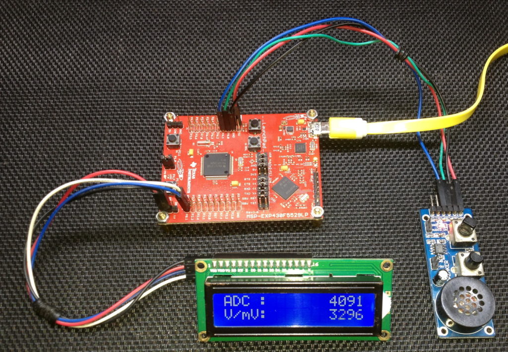
Hardware Setup
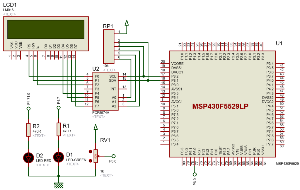
Explanation
ADC12 is configured just as we already did in past examples but no ADC12 interrupt is used. The new changes are related to DMA configuration. We wish to transfer ADC data to our designated memory location with DMA hardware. Thus, we have to declare a word-sized global variable. We chose word size, i.e. 16-bit because ADC12 readings are typically 12-bit in size. This memory location will be used with DMA and that makes it important.
uint16_t memory_location = 0x0000;
DMA initialization requires a few parameters to be set in order to define the its characteristics.
void DMA_HW_init(void)
{
    DMA_initParam DMA_init_Param = {0};

    DMA_disableTransferDuringReadModifyWrite();

    DMA_init_Param.channelSelect = DMA_CHANNEL_0;
    DMA_init_Param.transferModeSelect = DMA_TRANSFER_REPEATED_SINGLE;
    DMA_init_Param.transferSize = 1;
    DMA_init_Param.triggerSourceSelect = DMA_TRIGGERSOURCE_24;
    DMA_init_Param.transferUnitSelect = DMA_SIZE_SRCWORD_DSTWORD;
    DMA_init_Param.triggerTypeSelect = DMA_TRIGGER_RISINGEDGE;

    DMA_init(&DMA_init_Param);

    DMA_setSrcAddress(DMA_CHANNEL_0,
                      ADC12_A_getMemoryAddressForDMA(ADC12_A_BASE, ADC12_A_MEMORY_0),
                      DMA_DIRECTION_UNCHANGED);

    DMA_setDstAddress(DMA_CHANNEL_0,
                      (uint32_t)(uintptr_t)&memory_location,
                      DMA_DIRECTION_INCREMENT);

    DMA_clearInterrupt(DMA_CHANNEL_0);

    DMA_enableInterrupt(DMA_CHANNEL_0);

    DMA_enableTransfers(DMA_CHANNEL_0);

    __enable_interrupt();
}
The operation of DMA peripheral is similar to that of a water pipeline. In a water pipeline, we have to define source of water and its destination along with flow direction and frequency of flow. We also have to define the pipe size (diameter) in order to avoid unwanted fluid pressure, back-flow and water loss.
In similar terms, for a DMA peripheral, we have to define source and destination of data and the size of data. The source of data in this case is ADC12’s 0th memory location and the destination is the word-sized global variable we declared in the beginning of the code. We have to let the compiler know the physical addresses, i.e. pointer of the source and the destination.
MSP430’s DMA can support the following transfer modes:
We will be using 0th DMA channel in repeated single transfer mode since the ADC will be converting data repeatedly. The transfers will be in words and why it is so has already been explained.
Since we are using repeated single transfer mode, a trigger source is needed that will initiate the transfer. In this code, the DMA trigger source is numbered 24.
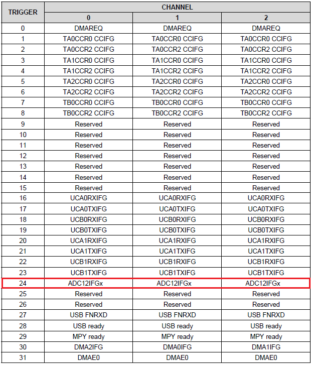
The 24th DMA trigger source is selected because we want the transfer to occur when an AD conversion is ready to be read.
Though DMA interrupt has been used in the code, it does nothing rather than toggling P1.0 LED. This is merely an indicator of data transfer completion.
#pragma vector = DMA_VECTOR
__interrupt void DMA_ISR (void)
{
    switch (__even_in_range(DMAIV, 16))
    {
        case 0: break;  //None
        case 2:         //DMA0IFG = DMA Channel 0
        {
            GPIO_toggleOutputOnPin(GPIO_PORT_P1, GPIO_PIN0);

            break;
        }
        case 4: break;  //DMA1IFG = DMA Channel 1
        case 6: break;  //DMA2IFG = DMA Channel 2
        case 8: break;  //DMA3IFG = DMA Channel 3
        case 10: break; //DMA4IFG = DMA Channel 4
        case 12: break; //DMA5IFG = DMA Channel 5
        case 14: break; //DMA6IFG = DMA Channel 6
        case 16: break; //DMA7IFG = DMA Channel 7
        default: break;
    }
}
In the main loop, the destination memory location is read. Both voltage and ADC count are displayed on an LCD. P4.7 LED is toggled to indicated that LCD data update and memory read have been done.
volt = ((memory_location * 3300.0) / 4095.0);

print_I(11, 0, memory_location);
print_I(11, 1, volt);

GPIO_toggleOutputOnPin(GPIO_PORT_P4, GPIO_PIN7);
delay_ms(200);
Note that in the code, we didn’t use any ADC12 function like the one shown below for reading the ADC.
ADC12_A_getResults(ADC12_A_BASE, ADC12_A_MEMORY_0);
We read the ADC indirectly using the DMA peripheral.
Demo
|
|
Hello, dear sir Shawon Shahryiar, could you send me the GRACE program by email? I can’t find it anywhere on the Internet. Thank you very much and all the best.
https://www.dropbox.com/scl/fi/6jgmxuuwl9dw2zo9mpuwm/grace_setup_2.2.0.00006.rar?rlkey=gm20hy3odiuyajjow2pas3iz0&st=hhfakdjt&dl=0
Hello, what software are you using for the Hardware setup images and does it support simulation for the MSP430F5529
I used Proteus VSM for drawing schematics but it doesn’t support simulation.
Hi,
Im interfacing MSP430F5529 with MAX17055 fuel guage. while reading 16 bit value, the first byte im receiving is 0. so while reading multiple registers continuously the data exchange is happening, but im getting the correct data. Can anyone suggest me what will be the issue? why im getting 0 in first byte?
read16_bit data code:
uint16_t value = 0;
USCI_B_I2C_setslaveaddress(USCI_B1_BASE, slave_address);
USCI_B_I2C_setmode(USCI_B1_BASE, USCI_B_I2C_TRANSMIT_MODE);
USCI_B_I2C_masterSendStart(USCI_B1_BASE);
while (!USCI_B_I2C_masterSendStart(USCI_B1_BASE));
USCI_B_I2C_mastterSendSingleByte(USCI_B1_BASE, reg_address);
USCI_B_I2C_setslaveaddress(USCI_B1_BASE, slave_address);
USCI_B_I2C_setmode(USCI_B1_BASE, USCI_B_I2C_TRANSMIT_MODE);
USCI_B_I2C_masterReceiveMultiByteStart(USCI_B1_BASE);
uint8_t lb = USCI_B_I2C_masterReceiveMultiByteNext(USCI_B1_BASE);
uint8_t hb = USCI_B_I2C_masterReceiveMultiByteFinish(USCI_B1_BASE);
while (USCI_B_I2C_isBusBusy(USCI_B_BASE));
value = lb << 8;
value |= hb;
return value;
In code, after sending reg address, it will be recieve mode. its a type mistake
Hi, im trying to send the command from the terminal view. i can able to send the command and tried to blink p1.0 led in msp430f5529 controller, its working fine. And im using led driver IS31FL3236A interfaced with msp430f5529 controller, i can able to interface im getting the expected output.
now i need to send the command from seriak monitor based on that command i2c communication need to start. both communication are working fine, when it runs separately. its not working when i tried to combine.
any one had any idea, why it is happening or what will be the issue?
It could be due to:
1. conflicts in clock settings
2. hardware conflict like pin mapping
3. code is getting stuck or waiting for one communication line to finish
4. use of polling method instead of interrupt-driven coding
Hi, thank you for the respose.
Do I need to use different clock initialization for I2C and UART communication? if YES, can you explain how to do that?
I mean check which clock has been set for UART and I2C…. Is it SMCLK, MCLK, etc and is it tuned to right frequency required by the respective hardware?
Is there any example on how to implement polling method in uart?
Why go for polling method when it is a blocking method of coding? It is better to use interrupts instead at least for UART receive.
yes!! currently in my code, only for uart im using interrupts to recieve command from serial monitor. Im not using interrupt for I2C communication.
so the issue is must be in clock initialization. right?
For UART, im using USCI_A1_BASE. and for I2C, im using USCI_B1_BASE.
And another thing i need to ask is, in uart when i tried blink led(p1.0) in msp430f5529 by passing command. here, without clock I’m getting output. how it is possible?
And for both i2c and uart i gave SMCLK with 1Mhz
I am surprised and happy to find this tutorial on the F5529 as TI makes a lot of different devices.
Thank you very much for putting in the extra knowledge in each segment, made reading worthwhile.
Good Work!
lovely tutorial but to be honest I don’t think I’d be investing my time on this board to start with it’s not cheap and readily available as the stm32 boards can you please do more tutorials on stm32 board’s and the stc micros thanks
Hello, I try to program MSP430FR6047 but i get error “the debug interface to the device has been secured”. when flashing using uniflash and when program using CCS this happen. can you help me to solve this problem
You can try “On connect, erase user code and unlock the device” option.
Pingback: Tinkering TI MSP430F5529 – gStore
Hello
I am doing project of msp430g2553 interface(using i2c communication) with temp 100(temperature sensor) and try to read the temperature in dispaly(16*2) but didn’t get the out put (using code composer studio) can u share me any example code for this project
Thank you sir,
Which sensor? Did you use pullup resistors for SDA-SCL pins?
Where is lcd_print.h?
All files and docs are here:
https://libstock.mikroe.com/projects/view/3233/tinkering-ti-msp430f5529
You want the truth? TI makes and sell “underpowered micros”, you know? Low everything, not only the power but also peripherals. So the price is not justified.
Otherwise, if I’ll move there, I’ll introduce them to my small hobby projects – there are still some advantages.
I may even make a visual configuration tool of my own for them…
Yeah the prices of TI products are higher than other manufacturers but I don’t think the hardware peripherals are inferior.
Not inferior but in not enough numbers compared to STM32.
True