Tinkering TI MSP430F5529
|
|
Internal Flash Memory and Cyclic Redundancy Check (CRC) Module
There are many microcontrollers in today’s market that don’t come with embedded EEPROM memory. Most ARM microcontrollers, for example, don’t have EEPROM memories. EEPROM is typically used for the storage of non-volatile data like configurations, calibrations, etc that are usually not changed frequently and need to be retained even after reset/power failure. EEPROM memories are slow and have lower endurance. Due to these limitations, it is better to use segments of flash memory that will not be used to hold application code. Flash memories have comparatively higher life cycles, high reliability and are faster. The only problem with them is writing. We can’t write to individual locations. We have to write/erase a whole segment of multiple byte areas at a time. No matter which memory class we are dealing with, frequent writing/erasing of memory locations also leads to wear and permanent damage. These issues can be avoided by a number of software-based means like wear-leveling. Data reading has no issues as data can be read individually or as a whole. MSP430F5529 has four flash memory areas called information memory (A to D). Information memory is where we can store non-volatile data and these locations have no conflict with application/main memory locations.
In MSP430F5529 micro, there is a Cyclic Redundancy Check (CRC) hardware. This hardware has several uses. Most commonly it is used to ensure or check data integrity against data corruption. In communications and data storage, CRC is highly needed since there is no other good and simple mean to cross-check data integrity efficiently and quickly.
CRC is like an agreement/encryption that two/more parties agree upon. As an example, consider two people, A and B sharing a common safe. A leaves a message in the safe for B. B has to open the safe with the same kind of key that A used to lock the safe or else B won’t get the message. Here the keys form the agreement that both of these persons agreed upon and the safe is the method to encapsulate the message from unwanted people.
Modern communication and data storage use CRC just like the example detailed above. CRC is an algorithm that tells dictates this encryption. Data is sent/stored along with a CRC code. When the sent/stored data is received/read along with the CRC content of the data, CRC is recalculated and verified against the sent/stored CRC. If both sent/stored CRC and received/read CRC match then it is safe to assume that no data corruption has occurred.
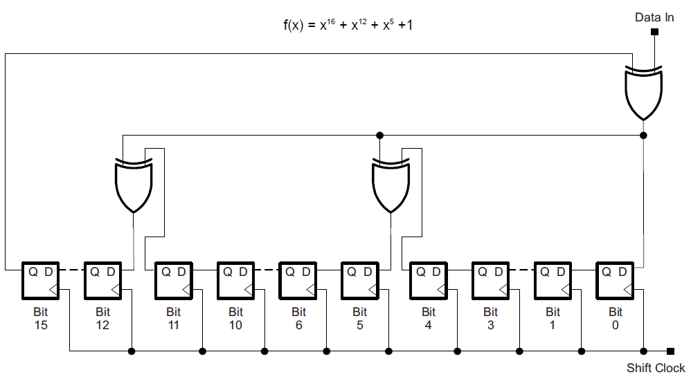
Shown below is the CRC module block diagram of MSP430F5529. The CRC module produces a signature for a given sequence of data values. The signature is generated through a feedback path from data bits 0, 4, 11, and 15. The CRC signature is based on the polynomial given in the CRC-CCITT-BR polynomial.
Code Example
#include "driverlib.h"
#include "delay.h"
#include "lcd.h"
#include "lcd_print.h"

#define INFOA_START     0x1980
#define INFOA_END       0x19FF

#define INFOB_START     0x1900
#define INFOB_END       0x197F

#define INFOC_START     0x1880
#define INFOC_END       0x18FF

#define INFOD_START     0x1800
#define INFOD_END       0x187F

void clock_init(void);
void GPIO_init(void);
char Flash_Read_Char(unsigned int address);
unsigned int Flash_Read_Word(unsigned int address);

void main(void)
{
    unsigned char s = 0x00;
    unsigned char temp = 0x00;
    unsigned char value[2] = {0x00, 0x00};
    unsigned char set_values[4] = {33, 64, 99, 16};
    unsigned int status = 0x0000;

    WDT_A_hold(WDT_A_BASE);

    clock_init();
    GPIO_init();

    LCD_init();
    LCD_clear_home();

    CRC_setSeed(CRC_BASE,
                0xABCD);

    CRC_set8BitData(CRC_BASE,
                    Flash_Read_Char(INFOB_START));

    temp = CRC_getResult(CRC_BASE);

    LCD_goto(0, 0);
    LCD_putstr("Checking CRC");

    LCD_goto(0, 1);
    LCD_putstr("STO");

    LCD_goto(8, 1);
    LCD_putstr("CRC");

    print_C(3, 1, Flash_Read_Char(INFOB_START + 1));
    print_C(11, 1, temp);

    delay_ms(1600);

    LCD_clear_home();

    LCD_goto(0, 0);
    LCD_putstr("INFO A Seg.");

    if(temp != Flash_Read_Char(INFOB_START + 1))
    {
        do
        {
            FlashCtl_eraseSegment((unsigned char *)INFOB_START);

            status = FlashCtl_performEraseCheck((unsigned char *)INFOB_START,
                                                128);
        }while (status == STATUS_FAIL);
    }

    if((GPIO_getInputPinValue(GPIO_PORT_P2,
                              GPIO_PIN1) == false))
    {
        GPIO_setOutputHighOnPin(GPIO_PORT_P4,
                                GPIO_PIN7);

        FlashCtl_unlockInfoA();

        do
        {
            FlashCtl_eraseSegment((unsigned char *)INFOA_START);

            status = FlashCtl_performEraseCheck((unsigned char *)INFOA_START,
                                                128);
        }while (status == STATUS_FAIL);

        FlashCtl_write8(set_values,
                        (unsigned char *)INFOA_START,
                        4);

        FlashCtl_lockInfoA();

        LCD_goto(0, 1);
        LCD_putstr("Set: 33 64 99 16");

        delay_ms(3000);

        GPIO_setOutputLowOnPin(GPIO_PORT_P4,
                               GPIO_PIN7);
    }

    else
    {
        LCD_goto(0, 1);
        LCD_putstr("Read");

        for(s = 0; s < 4; s++)
        {
            temp = Flash_Read_Char(INFOA_START + s);
            print_C(5, 1, s);
            print_C(13, 1, temp);
            delay_ms(2000);
        }
    }

    LCD_clear_home();

    LCD_goto(0, 0);
    LCD_putstr("INFO B Seg.");

    temp = Flash_Read_Char(INFOB_START);
    LCD_goto(0, 1);
    LCD_putstr("WR: ---");
    LCD_goto(9, 1);
    LCD_putstr("RD:");
    print_C(12, 1, temp);
    delay_ms(2000);

    temp = 0;

    while(1)
    {
        if(GPIO_getInputPinValue(GPIO_PORT_P1,
                                 GPIO_PIN1) == false)
        {
            while(GPIO_getInputPinValue(GPIO_PORT_P1,
                                        GPIO_PIN1) == false);

            print_C(3, 1, value[0]);

            do
            {
                FlashCtl_eraseSegment((unsigned char *)INFOB_START);

                status = FlashCtl_performEraseCheck((unsigned char *)INFOB_START,
                                                    128);
            }while (status == STATUS_FAIL);

            CRC_setSeed(CRC_BASE,
                        0xABCD);

            CRC_set8BitData(CRC_BASE,
                            value[0]);

            value[1] = CRC_getResult(CRC_BASE);

            FlashCtl_write8(value,
                            (unsigned char *)INFOB_START,
                            2);

            GPIO_setOutputHighOnPin(GPIO_PORT_P4,
                                    GPIO_PIN7);

            delay_ms(1000);

            GPIO_setOutputLowOnPin(GPIO_PORT_P4,
                                   GPIO_PIN7);

        }

        delay_ms(20);

        print_C(3, 1, value[0]);
        value[0] = temp++;

        delay_ms(200);
    };
}

void clock_init(void)
{
    PMM_setVCore(PMM_CORE_LEVEL_3);

    GPIO_setAsPeripheralModuleFunctionInputPin(GPIO_PORT_P5,
                                               (GPIO_PIN4 | GPIO_PIN2));

    GPIO_setAsPeripheralModuleFunctionOutputPin(GPIO_PORT_P5,
                                                (GPIO_PIN5 | GPIO_PIN3));

    UCS_setExternalClockSource(XT1_FREQ,
                               XT2_FREQ);

    UCS_turnOnXT2(UCS_XT2_DRIVE_4MHZ_8MHZ);

    UCS_turnOnLFXT1(UCS_XT1_DRIVE_3,
                    UCS_XCAP_3);

    UCS_initClockSignal(UCS_FLLREF,
                        UCS_XT2CLK_SELECT,
                        UCS_CLOCK_DIVIDER_4);

    UCS_initFLLSettle(MCLK_KHZ,
                      MCLK_FLLREF_RATIO);

    UCS_initClockSignal(UCS_SMCLK,
                        UCS_XT2CLK_SELECT,
                        UCS_CLOCK_DIVIDER_2);

    UCS_initClockSignal(UCS_ACLK,
                        UCS_XT1CLK_SELECT,
                        UCS_CLOCK_DIVIDER_1);
}

void GPIO_init(void)
{
    GPIO_setAsInputPinWithPullUpResistor(GPIO_PORT_P1,
                                         GPIO_PIN1);

    GPIO_setAsInputPinWithPullUpResistor(GPIO_PORT_P2,
                                         GPIO_PIN1);

    GPIO_setAsOutputPin(GPIO_PORT_P1,
                        GPIO_PIN0);

    GPIO_setDriveStrength(GPIO_PORT_P1,
                          GPIO_PIN0,
                          GPIO_FULL_OUTPUT_DRIVE_STRENGTH);

    GPIO_setAsOutputPin(GPIO_PORT_P4,
                        GPIO_PIN7);

    GPIO_setDriveStrength(GPIO_PORT_P4,
                          GPIO_PIN7,
                          GPIO_FULL_OUTPUT_DRIVE_STRENGTH);
}

char Flash_Read_Char(unsigned int address)
{
    char value = 0x00;
    char *FlashPtr = (char *)address;

    value = *FlashPtr;

    return value;
}

unsigned int Flash_Read_Word(unsigned int address)
{
    unsigned int value = 0x0000;
    unsigned int *FlashPtr = (unsigned int *)address;

    value = *FlashPtr;

    return value;
}
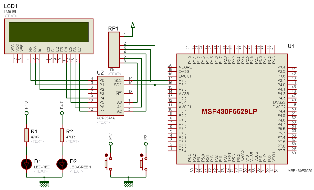
Hardware Setup
Explanation
The idea here is to use internal flash memory for storing non-volatile user data and CRC module for verification of data integrity.
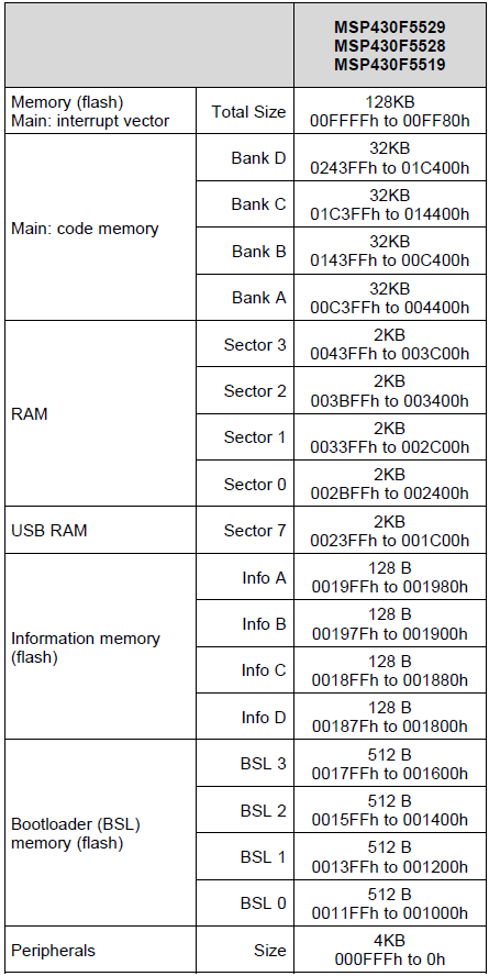
MSP430F5529’s flash memory is partitioned into main, information, and BSL memory sections. The main flash memory is used for storing application code, BSL memory is used for storing bootloader and the information memory is used for storing non-volatile user data. Check the memory map shown below. Here two out of three types of flash memories are shown only. Different sizes of data can be read/written in flash memory but when erasing only segment-sized erase is possible. The segment size of main and BSL memories is 512 bytes and the segment size of information memories is 128 bytes. Since information memory segments are smaller than other flash memories, it is best suited for user data storage for obvious memory segment size advantage. Lesser size means faster operation, lesser wear and efficient memory management. As mentioned before, frequent writes/erases wear memories and so it is a good practice not do either frequently. Complex software-based wear-levelling techniques and using RAM-backed buffers can be applied to reduce memory wears.
Segment A is a very important segment as it can be used to stores important/critical internal calibration data, configurations and other important set points. This is why, it is protected and locked separately. It is wise to leave it and use the other three segments of information memory space to store user data that frequently change.
Now let’s see how the code works here.
Firstly, let us start by defining the location boundaries of the information memory segments.
#define INFOA_START     0x1980
#define INFOA_END       0x19FF

#define INFOB_START     0x1900
#define INFOB_END       0x197F

#define INFOC_START     0x1880
#define INFOC_END       0x18FF

#define INFOD_START     0x1800
#define INFOD_END       0x187F
CRC check is done in the beginning of the code although at first run CRC check is invalid as no user data is initially stored. However, this comes to use when we reset or power up after saving our data.
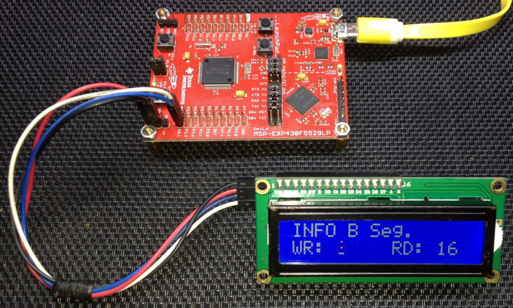
For CRC module to work, we need to give a seed, i.e. a number in form of a key. Here it is arbitrarily set as 0XABCD. CRC module uses this seed and given data to compute CRC result. After this we visually check if the stored CRC matches with the calculated CRC. The check is done in code too. The CRC values are stored in two locations of the B segment of information memory.
CRC_setSeed(CRC_BASE, 0xABCD);

CRC_set8BitData(CRC_BASE, Flash_Read_Char(INFOB_START));

temp = CRC_getResult(CRC_BASE);

LCD_goto(0, 0);
LCD_putstr("Checking CRC");

LCD_goto(0, 1);
LCD_putstr("STO");

LCD_goto(8, 1);
LCD_putstr("CRC");

print_C(3, 1, Flash_Read_Char(INFOB_START + 1));
print_C(11, 1, temp);


delay_ms(1600);

LCD_clear_home();

LCD_goto(0, 0);
LCD_putstr("INFO A Seg.");

if(temp != Flash_Read_Char(INFOB_START + 1))
{
    do
    {
        FlashCtl_eraseSegment((unsigned char *)INFOB_START);

        status = FlashCtl_performEraseCheck((unsigned char *)INFOB_START,
                                             128);
     }while(status == STATUS_FAIL);
}
If the contents of both locations of Info B memory are different then it is likely that the memories are corrupt/empty and so an erase cycle is necessary to wipe out inconsistent data. The entire Info B segment is erased. If it is otherwise then the erase is not performed.
Now let us put some simulated fixed data as if these data are set points of some process or hardware. To set these data in Info A memory we have to push P2.1 button. First, the segment is unlocked and then an erase is performed to get rid of old data. After the erase cycle, data (array named “set_values”) is stored and the flash segment is locked. The locking ensures that no other operation is possible with this memory unless unlocked.
If the P2.1 button is not pressed then stored data is simply read.
Note no CRC check is performed for this segment.
if((GPIO_getInputPinValue(GPIO_PORT_P2, GPIO_PIN1) == false))
{
    GPIO_setOutputHighOnPin(GPIO_PORT_P4, GPIO_PIN7);

    FlashCtl_unlockInfoA();

    do
    {
       FlashCtl_eraseSegment((unsigned char *)INFOA_START);

       status = FlashCtl_performEraseCheck((unsigned char *)INFOA_START, 128);
     }while (status == STATUS_FAIL);

     FlashCtl_write8(set_values, (unsigned char *)INFOA_START, 4);

     FlashCtl_lockInfoA();

     LCD_goto(0, 1);
     LCD_putstr("Set: 33 64 99 16");

     delay_ms(2600);

     GPIO_setOutputLowOnPin(GPIO_PORT_P4, GPIO_PIN7);
    }

else
{
    LCD_goto(0, 1);
    LCD_putstr("Read");

    for(s = 0; s < 4; s++)
    {
        temp = Flash_Read_Char(INFOA_START + s);
        print_C(5, 1, s);
        print_C(13, 1, temp);
        delay_ms(2000);
    }
}
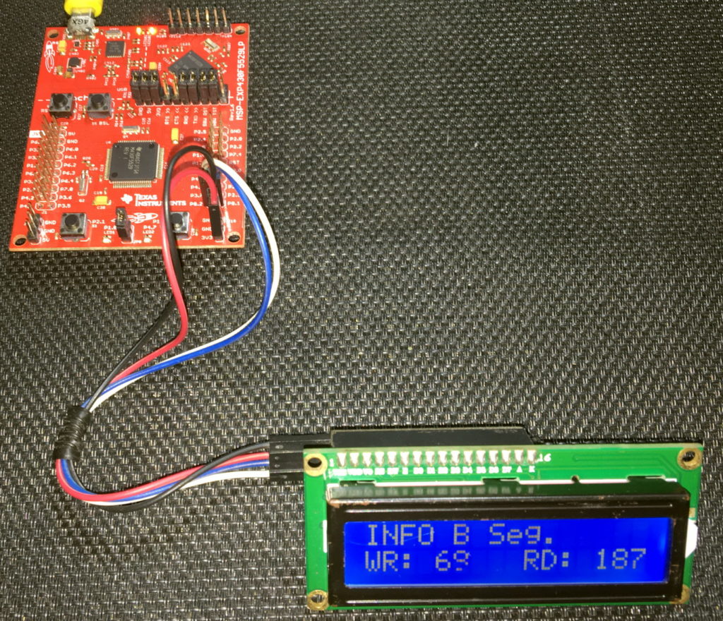
All of the tasks mentioned so far are done before the main loop. In the main loop a value named “temp” is incremented. When P1.1 button is pressed, the current value of temp is stored in Info B segment. Since we cannot rewrite or overwrite a flash memory, we must perform an erase operation before storing new data. When a new data is stored, a CRC is also performed with 0xABCD as seed as in the beginning of the code. The new data and CRC are saved in two different locations. These two values will be used for checking data integrity when the MSP430 micro resets or powers up next. This is what we saw at the beginning of the code.
Note that there is no Info B locking unlocking feature.
if(GPIO_getInputPinValue(GPIO_PORT_P1, GPIO_PIN1) == false)
{
   while(GPIO_getInputPinValue(GPIO_PORT_P1, GPIO_PIN1) == false);

   print_C(3, 1, value[0]);

   do
   {
       FlashCtl_eraseSegment((unsigned char *)INFOB_START);

       status = FlashCtl_performEraseCheck((unsigned char *)INFOB_START, 128);
    }while (status == STATUS_FAIL);

    CRC_setSeed(CRC_BASE, 0xABCD);

    CRC_set8BitData(CRC_BASE, value[0]);

    value[1] = CRC_getResult(CRC_BASE);

    FlashCtl_write8(value, (unsigned char *)INFOB_START, 2);

    GPIO_setOutputHighOnPin(GPIO_PORT_P4, GPIO_PIN7);

    delay_ms(1000);

    GPIO_setOutputLowOnPin(GPIO_PORT_P4, GPIO_PIN7);
}

delay_ms(20);

print_C(3, 1, value[0]);
value[0] = temp++;

delay_ms(200);
Demo

|
|
Hello, dear sir Shawon Shahryiar, could you send me the GRACE program by email? I can’t find it anywhere on the Internet. Thank you very much and all the best.
https://www.dropbox.com/scl/fi/6jgmxuuwl9dw2zo9mpuwm/grace_setup_2.2.0.00006.rar?rlkey=gm20hy3odiuyajjow2pas3iz0&st=hhfakdjt&dl=0
Hello, what software are you using for the Hardware setup images and does it support simulation for the MSP430F5529
I used Proteus VSM for drawing schematics but it doesn’t support simulation.
Hi,
Im interfacing MSP430F5529 with MAX17055 fuel guage. while reading 16 bit value, the first byte im receiving is 0. so while reading multiple registers continuously the data exchange is happening, but im getting the correct data. Can anyone suggest me what will be the issue? why im getting 0 in first byte?
read16_bit data code:
uint16_t value = 0;
USCI_B_I2C_setslaveaddress(USCI_B1_BASE, slave_address);
USCI_B_I2C_setmode(USCI_B1_BASE, USCI_B_I2C_TRANSMIT_MODE);
USCI_B_I2C_masterSendStart(USCI_B1_BASE);
while (!USCI_B_I2C_masterSendStart(USCI_B1_BASE));
USCI_B_I2C_mastterSendSingleByte(USCI_B1_BASE, reg_address);
USCI_B_I2C_setslaveaddress(USCI_B1_BASE, slave_address);
USCI_B_I2C_setmode(USCI_B1_BASE, USCI_B_I2C_TRANSMIT_MODE);
USCI_B_I2C_masterReceiveMultiByteStart(USCI_B1_BASE);
uint8_t lb = USCI_B_I2C_masterReceiveMultiByteNext(USCI_B1_BASE);
uint8_t hb = USCI_B_I2C_masterReceiveMultiByteFinish(USCI_B1_BASE);
while (USCI_B_I2C_isBusBusy(USCI_B_BASE));
value = lb << 8;
value |= hb;
return value;
In code, after sending reg address, it will be recieve mode. its a type mistake
Hi, im trying to send the command from the terminal view. i can able to send the command and tried to blink p1.0 led in msp430f5529 controller, its working fine. And im using led driver IS31FL3236A interfaced with msp430f5529 controller, i can able to interface im getting the expected output.
now i need to send the command from seriak monitor based on that command i2c communication need to start. both communication are working fine, when it runs separately. its not working when i tried to combine.
any one had any idea, why it is happening or what will be the issue?
It could be due to:
1. conflicts in clock settings
2. hardware conflict like pin mapping
3. code is getting stuck or waiting for one communication line to finish
4. use of polling method instead of interrupt-driven coding
Hi, thank you for the respose.
Do I need to use different clock initialization for I2C and UART communication? if YES, can you explain how to do that?
I mean check which clock has been set for UART and I2C…. Is it SMCLK, MCLK, etc and is it tuned to right frequency required by the respective hardware?
Is there any example on how to implement polling method in uart?
Why go for polling method when it is a blocking method of coding? It is better to use interrupts instead at least for UART receive.
yes!! currently in my code, only for uart im using interrupts to recieve command from serial monitor. Im not using interrupt for I2C communication.
so the issue is must be in clock initialization. right?
For UART, im using USCI_A1_BASE. and for I2C, im using USCI_B1_BASE.
And another thing i need to ask is, in uart when i tried blink led(p1.0) in msp430f5529 by passing command. here, without clock I’m getting output. how it is possible?
And for both i2c and uart i gave SMCLK with 1Mhz
I am surprised and happy to find this tutorial on the F5529 as TI makes a lot of different devices.
Thank you very much for putting in the extra knowledge in each segment, made reading worthwhile.
Good Work!
lovely tutorial but to be honest I don’t think I’d be investing my time on this board to start with it’s not cheap and readily available as the stm32 boards can you please do more tutorials on stm32 board’s and the stc micros thanks
Hello, I try to program MSP430FR6047 but i get error “the debug interface to the device has been secured”. when flashing using uniflash and when program using CCS this happen. can you help me to solve this problem
You can try “On connect, erase user code and unlock the device” option.
Pingback: Tinkering TI MSP430F5529 – gStore
Hello
I am doing project of msp430g2553 interface(using i2c communication) with temp 100(temperature sensor) and try to read the temperature in dispaly(16*2) but didn’t get the out put (using code composer studio) can u share me any example code for this project
Thank you sir,
Which sensor? Did you use pullup resistors for SDA-SCL pins?
Where is lcd_print.h?
All files and docs are here:
https://libstock.mikroe.com/projects/view/3233/tinkering-ti-msp430f5529
You want the truth? TI makes and sell “underpowered micros”, you know? Low everything, not only the power but also peripherals. So the price is not justified.
Otherwise, if I’ll move there, I’ll introduce them to my small hobby projects – there are still some advantages.
I may even make a visual configuration tool of my own for them…
Yeah the prices of TI products are higher than other manufacturers but I don’t think the hardware peripherals are inferior.
Not inferior but in not enough numbers compared to STM32.
True