Tinkering TI MSP430F5529
|
|
REF Module and ADC12 in Polling Mode
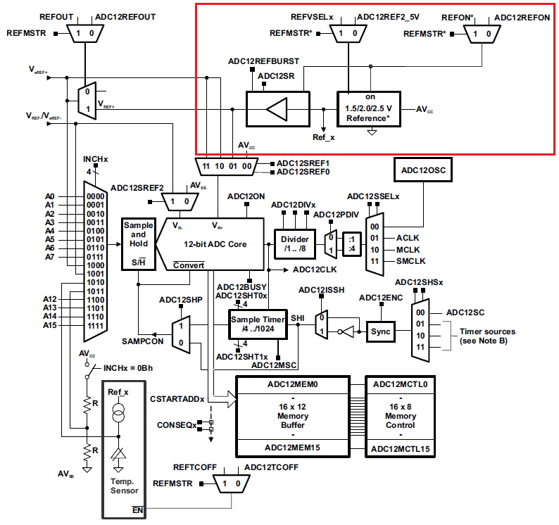
Good ADC performance and accurate readings depend on good reference sources. The stable these reference sources are with respect to changes in temperature and input voltage fluctuations, the better the ADC readings. MSP430F5529 is equipped with a built-in reference source generator module called REF module that is able to generate 1.5V, 2.0V and 2.5V with good precision. REF module has good temperature coefficients and power-saving features. REF module doesn’t restrict us from using external reference sources but since they are available internally and factory trimmed, it is better to use them to reduce external parts count and avoid unnecessary hassle. The highlighted region in ADC12’s block diagram shown below shows the components of MSP430F5529’s REF module. A quick view reveals how they are connected with the ADC.
ADC12 is perhaps simply understood without the use of DMA and interrupts. ADC12 is configured and started. Readings of ADC channels are stored in ADC memory locations after conversions. Reading ADC memories give out last conversion results. In this example, we will see exactly that and we will be reading MSP430’s internal temperature sensor with the ADC.
Code Example
#include "driverlib.h"
#include "delay.h"
#include "lcd.h"
#include "lcd_print.h"

void clock_init(void);
void GPIO_init(void);
void ADC12_init(void);
void REF_init(void);

void main(void)
{
    signed int ADC_Count = 0;
    signed long temp = 0;

    WDT_A_hold(WDT_A_BASE);

    clock_init();
    GPIO_init();
    REF_init();
    ADC12_init();

    LCD_init();
    LCD_clear_home();
    load_custom_symbol();

    LCD_goto(0, 0);
    LCD_putstr("ADC :");

    LCD_goto(0, 1);
    LCD_putstr("T/ C:");
    print_symbol(2, 1, 0);

    while(1)
    {
        ADC_Count = ADC12_A_getResults(ADC12_A_BASE,
                                       ADC12_A_MEMORY_0);

        temp = ((((signed long)ADC_Count - 1855) * 667) / 4096);

        print_I(11, 0, ADC_Count);
        print_I(13, 1, temp);

        delay_ms(200);
    };
}

void clock_init(void)
{
    PMM_setVCore(PMM_CORE_LEVEL_3);

    GPIO_setAsPeripheralModuleFunctionInputPin(GPIO_PORT_P5,
                                               (GPIO_PIN4 | GPIO_PIN2));

    GPIO_setAsPeripheralModuleFunctionOutputPin(GPIO_PORT_P5,
                                                (GPIO_PIN5 | GPIO_PIN3));

    UCS_setExternalClockSource(XT1_FREQ,
                               XT2_FREQ);

    UCS_turnOnXT2(UCS_XT2_DRIVE_4MHZ_8MHZ);

    UCS_turnOnLFXT1(UCS_XT1_DRIVE_0,
                    UCS_XCAP_3);

    UCS_initClockSignal(UCS_FLLREF,
                        UCS_XT2CLK_SELECT,
                        UCS_CLOCK_DIVIDER_4);

    UCS_initFLLSettle(MCLK_KHZ,
                      MCLK_FLLREF_RATIO);

    UCS_initClockSignal(UCS_SMCLK,
                        UCS_XT2CLK_SELECT,
                        UCS_CLOCK_DIVIDER_2);

    UCS_initClockSignal(UCS_ACLK,
                        UCS_XT1CLK_SELECT,
                        UCS_CLOCK_DIVIDER_1);
}

void GPIO_init(void)
{
    GPIO_setAsOutputPin(GPIO_PORT_P4,
                        GPIO_PIN7);
}


void ADC12_init(void)
{
    ADC12_A_configureMemoryParam configureMemoryParam = {0};

    ADC12_A_init(ADC12_A_BASE,
                 ADC12_A_SAMPLEHOLDSOURCE_SC,
                 ADC12_A_CLOCKSOURCE_ACLK,
                 ADC12_A_CLOCKDIVIDER_1);

    ADC12_A_setupSamplingTimer(ADC12_A_BASE,
                               ADC12_A_CYCLEHOLD_768_CYCLES,
                               ADC12_A_CYCLEHOLD_4_CYCLES,
                               ADC12_A_MULTIPLESAMPLESENABLE);

    ADC12_A_setResolution(ADC12_A_BASE,
                          ADC12_A_RESOLUTION_12BIT);

    configureMemoryParam.memoryBufferControlIndex = ADC12_A_MEMORY_0;
    configureMemoryParam.inputSourceSelect = ADC12_A_INPUT_TEMPSENSOR;
    configureMemoryParam.positiveRefVoltageSourceSelect = ADC12_A_VREFPOS_INT;
    configureMemoryParam.negativeRefVoltageSourceSelect = ADC12_A_VREFNEG_AVSS;
    configureMemoryParam.endOfSequence = ADC12_A_NOTENDOFSEQUENCE;

    ADC12_A_configureMemory(ADC12_A_BASE,
                            &configureMemoryParam);

    ADC12_A_enable(ADC12_A_BASE);

    ADC12_A_startConversion(ADC12_A_BASE,
                            ADC12_A_MEMORY_0,
                            ADC12_A_REPEATED_SINGLECHANNEL);
}

void REF_init(void)
{
    while(REF_ACTIVE == Ref_isRefGenBusy(REF_BASE));

    Ref_setReferenceVoltage(REF_BASE,
                            REF_VREF1_5V);

    Ref_enableReferenceVoltage(REF_BASE);

    __delay_cycles(100);
}
Hardware Setup
Explanation
Let’s see first how the REF module is configured. REF module is not clock dependent as like other hardware and doesn’t require use of any external pin.
void REF_init(void)
{
    while(REF_ACTIVE == Ref_isRefGenBusy(REF_BASE));
    Ref_setReferenceVoltage(REF_BASE, REF_VREF1_5V);
    Ref_enableReferenceVoltage(REF_BASE);
    __delay_cycles(100);
}
Using REF module is very easy. We first check its state. We set our desired reference voltage. Here we need the 1.5V reference. After selection, we enable it and wait for some time to get it settled.
void ADC12_init(void)
{
    ADC12_A_configureMemoryParam configureMemoryParam = {0};

    ADC12_A_init(ADC12_A_BASE,
                 ADC12_A_SAMPLEHOLDSOURCE_SC,
                 ADC12_A_CLOCKSOURCE_ACLK,
                 ADC12_A_CLOCKDIVIDER_1);

    ADC12_A_setupSamplingTimer(ADC12_A_BASE,
                               ADC12_A_CYCLEHOLD_768_CYCLES,
                               ADC12_A_CYCLEHOLD_4_CYCLES,
                               ADC12_A_MULTIPLESAMPLESENABLE);

    ADC12_A_setResolution(ADC12_A_BASE, ADC12_A_RESOLUTION_12BIT);

    configureMemoryParam.memoryBufferControlIndex = ADC12_A_MEMORY_0;
    configureMemoryParam.inputSourceSelect = ADC12_A_INPUT_TEMPSENSOR;
    configureMemoryParam.positiveRefVoltageSourceSelect = ADC12_A_VREFPOS_INT;
    configureMemoryParam.negativeRefVoltageSourceSelect =                                      ADC12_A_VREFNEG_AVSS;
    configureMemoryParam.endOfSequence = ADC12_A_NOTENDOFSEQUENCE;

    ADC12_A_configureMemory(ADC12_A_BASE, &configureMemoryParam);

    ADC12_A_enable(ADC12_A_BASE);

    ADC12_A_startConversion(ADC12_A_BASE,
                            ADC12_A_MEMORY_0,
                            ADC12_A_REPEATED_SINGLECHANNEL);
}
We are not using any external channel and so there is no special pin setup for ADC12. As with any hardware, the source of ADC12’s clock is set first. Here the clock source is unscaled ACLK.
UCS_initClockSignal(UCS_ACLK, UCS_XT1CLK_SELECT, UCS_CLOCK_DIVIDER_1);
ACLK is fed with an external 32.768 kHz XT1 crystal running at 32.768 kHz.
Next, we set the sampling timer by defining the sample-hold times. We also set the ADC’s resolution to 12 bits. We can also set 8 and 10 resolution if required.
We also have to let the ADC know which ADC channel to read, where to store the readings and what the reference voltages are for the ADC block. Note that the reference voltage source is the 1.5V source.
We, finally, start the ADC and leave it in repeated single channel conversion mode. In this way, the ADC will continuously measure our desired channel and store readings in an ADC memory location (here Memory 0).
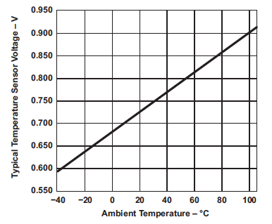
From the graph shown above, we can see that the voltage (ultimately ADC count) vs temperature relationship of the internal temperature sensor is a perfect straight-line and so a linear equation will be needed to describe this relationship. Now if we know the ADC count of the internal temperature sensor, we can determine MSP430’s core temperature.
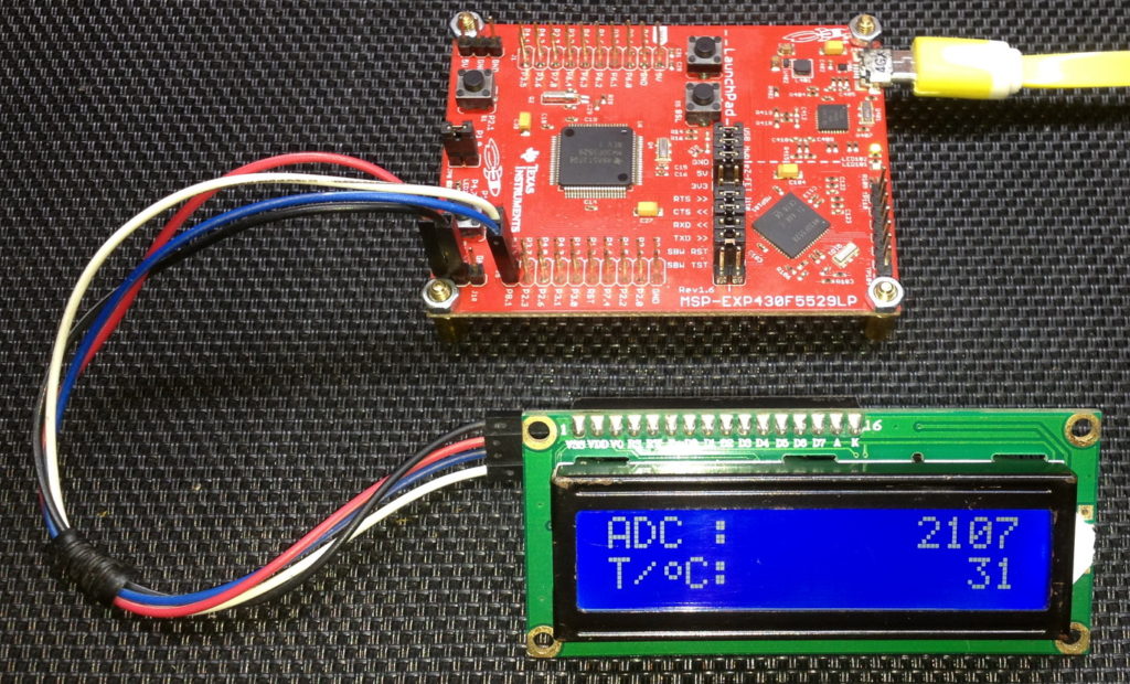
In the main loop, as I stated earlier, ADC memory 0 location is read and the reading is converted to temperature. The ADC count and the temperature are then shown on an LCD display.
ADC_Count = ADC12_A_getResults(ADC12_A_BASE, ADC12_A_MEMORY_0);

temp = ((((signed long)ADC_Count - 1855) * 667) / 4096);
Demo
|
|
Hello, what software are you using for the Hardware setup images and does it support simulation for the MSP430F5529
I used Proteus VSM for drawing schematics but it doesn’t support simulation.
Hi,
Im interfacing MSP430F5529 with MAX17055 fuel guage. while reading 16 bit value, the first byte im receiving is 0. so while reading multiple registers continuously the data exchange is happening, but im getting the correct data. Can anyone suggest me what will be the issue? why im getting 0 in first byte?
read16_bit data code:
uint16_t value = 0;
USCI_B_I2C_setslaveaddress(USCI_B1_BASE, slave_address);
USCI_B_I2C_setmode(USCI_B1_BASE, USCI_B_I2C_TRANSMIT_MODE);
USCI_B_I2C_masterSendStart(USCI_B1_BASE);
while (!USCI_B_I2C_masterSendStart(USCI_B1_BASE));
USCI_B_I2C_mastterSendSingleByte(USCI_B1_BASE, reg_address);
USCI_B_I2C_setslaveaddress(USCI_B1_BASE, slave_address);
USCI_B_I2C_setmode(USCI_B1_BASE, USCI_B_I2C_TRANSMIT_MODE);
USCI_B_I2C_masterReceiveMultiByteStart(USCI_B1_BASE);
uint8_t lb = USCI_B_I2C_masterReceiveMultiByteNext(USCI_B1_BASE);
uint8_t hb = USCI_B_I2C_masterReceiveMultiByteFinish(USCI_B1_BASE);
while (USCI_B_I2C_isBusBusy(USCI_B_BASE));
value = lb << 8;
value |= hb;
return value;
In code, after sending reg address, it will be recieve mode. its a type mistake
Hi, im trying to send the command from the terminal view. i can able to send the command and tried to blink p1.0 led in msp430f5529 controller, its working fine. And im using led driver IS31FL3236A interfaced with msp430f5529 controller, i can able to interface im getting the expected output.
now i need to send the command from seriak monitor based on that command i2c communication need to start. both communication are working fine, when it runs separately. its not working when i tried to combine.
any one had any idea, why it is happening or what will be the issue?
It could be due to:
1. conflicts in clock settings
2. hardware conflict like pin mapping
3. code is getting stuck or waiting for one communication line to finish
4. use of polling method instead of interrupt-driven coding
Hi, thank you for the respose.
Do I need to use different clock initialization for I2C and UART communication? if YES, can you explain how to do that?
I mean check which clock has been set for UART and I2C…. Is it SMCLK, MCLK, etc and is it tuned to right frequency required by the respective hardware?
Is there any example on how to implement polling method in uart?
Why go for polling method when it is a blocking method of coding? It is better to use interrupts instead at least for UART receive.
yes!! currently in my code, only for uart im using interrupts to recieve command from serial monitor. Im not using interrupt for I2C communication.
so the issue is must be in clock initialization. right?
For UART, im using USCI_A1_BASE. and for I2C, im using USCI_B1_BASE.
And another thing i need to ask is, in uart when i tried blink led(p1.0) in msp430f5529 by passing command. here, without clock I’m getting output. how it is possible?
And for both i2c and uart i gave SMCLK with 1Mhz
I am surprised and happy to find this tutorial on the F5529 as TI makes a lot of different devices.
Thank you very much for putting in the extra knowledge in each segment, made reading worthwhile.
Good Work!
lovely tutorial but to be honest I don’t think I’d be investing my time on this board to start with it’s not cheap and readily available as the stm32 boards can you please do more tutorials on stm32 board’s and the stc micros thanks
Hello, I try to program MSP430FR6047 but i get error “the debug interface to the device has been secured”. when flashing using uniflash and when program using CCS this happen. can you help me to solve this problem
You can try “On connect, erase user code and unlock the device” option.
Pingback: Tinkering TI MSP430F5529 – gStore
Hello
I am doing project of msp430g2553 interface(using i2c communication) with temp 100(temperature sensor) and try to read the temperature in dispaly(16*2) but didn’t get the out put (using code composer studio) can u share me any example code for this project
Thank you sir,
Which sensor? Did you use pullup resistors for SDA-SCL pins?
Where is lcd_print.h?
All files and docs are here:
https://libstock.mikroe.com/projects/view/3233/tinkering-ti-msp430f5529
You want the truth? TI makes and sell “underpowered micros”, you know? Low everything, not only the power but also peripherals. So the price is not justified.
Otherwise, if I’ll move there, I’ll introduce them to my small hobby projects – there are still some advantages.
I may even make a visual configuration tool of my own for them…
Yeah the prices of TI products are higher than other manufacturers but I don’t think the hardware peripherals are inferior.
Not inferior but in not enough numbers compared to STM32.
True