Mastering the SiLabs C8051 Microcontroller
|
|
General Purpose Input-Output (GPIO) and Clock System
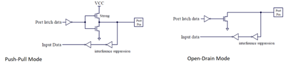
Playing with the GPIOs of C8051 microcontrollers is very easy. GPIOs can be either open-drain inputs and push-pull type outputs. The arrangements are simply as shown below:
The general block diagram for a C8051 GPIO pin is shown below:
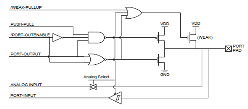
This arrangement is typical for all 8051-based microcontrollers. The subtle differences are the Schmitt-trigger and analogue input channels.
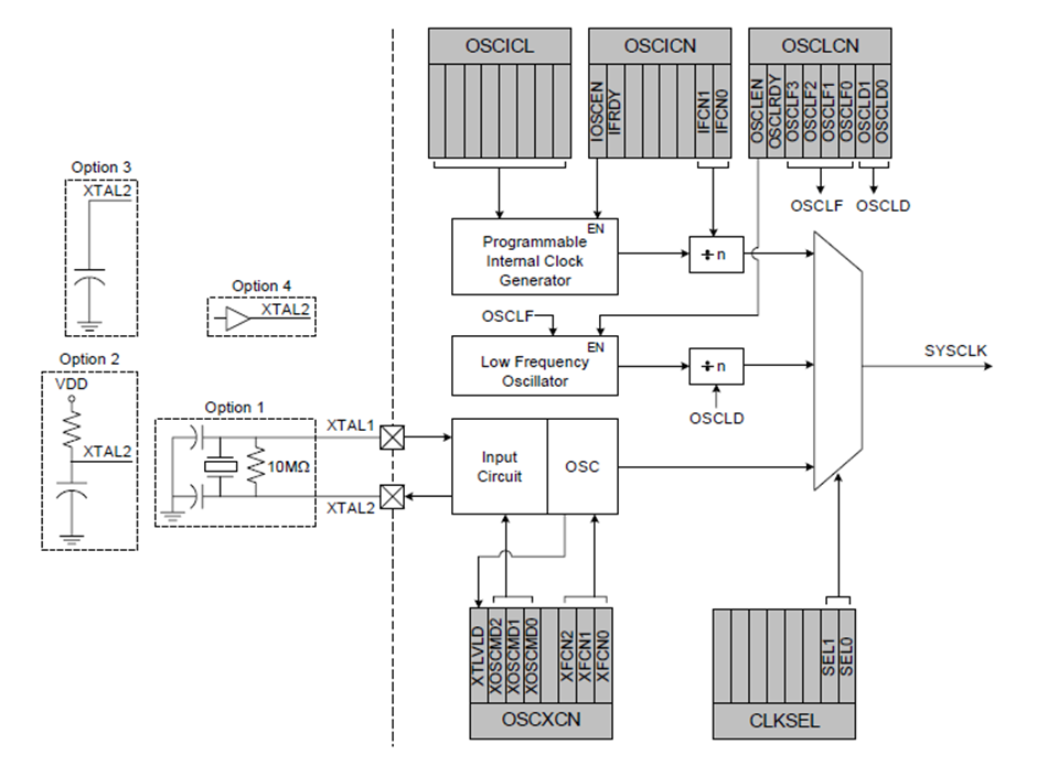
The clock system is also pretty straightforward. There is only one system clock and it can be fed with several clock sources. These include the internal low-frequency low accuracy oscillator, the programmable high-frequency internal clock generator or an external clock source which can be anything from a crystal oscillator to simple RC oscillators. Faster clocks are needed for fast data processing while slower clocks are intended for low power consumption. To vary clock speed, there are also clock dividers to scale clock sources according to requirement. All of these can be set in code. Refer to the block diagram below:
Code
 void PCA_Init(void);
 void Port_IO_Init(void);
 void Init_Device(void);

 void main(void)
 {
     unsigned char i = 0;

     Init_Device();

     P1_0_bit = 1;
     P1_1_bit = 0;

     while(1)
     {
        if(P1_4_bit == 0)
        {
            delay_ms(100);
            i++;
        }

        switch(i)
        {
            case 0:
            {
                OSCICN = 0x83;
                break;
            }
            case 1:
            {
                OSCICN = 0x82;
                break;
            }
            case 2:
            {
                OSCICN = 0x81;
                break;
            }
            case 3:
            {
                OSCICN = 0x80;
                break;
            }
            default:
            {
                i = 0;
                break;
            }
        }

        P1_0_bit ^= 1;
        P1_1_bit ^= 1;
        delay_ms(100);
     };
 }

 void PCA_Init(void)
 {
     PCA0MD &= ~0x40;
     PCA0MD = 0x00;
 }

 void Port_IO_Init(void)
 {
     // P0.0  -  Unassigned,  Open-Drain, Digital
     // P0.1  -  Unassigned,  Open-Drain, Digital
     // P0.2  -  Unassigned,  Open-Drain, Digital
     // P0.3  -  Unassigned,  Open-Drain, Digital
     // P0.4  -  Unassigned,  Open-Drain, Digital
     // P0.5  -  Unassigned,  Open-Drain, Digital
     // P0.6  -  Unassigned,  Open-Drain, Digital
     // P0.7  -  Unassigned,  Open-Drain, Digital

     // P1.0  -  Skipped,     Push-Pull,  Digital
     // P1.1  -  Skipped,     Push-Pull,  Digital
     // P1.2  -  Unassigned,  Open-Drain, Digital
     // P1.3  -  Unassigned,  Open-Drain, Digital
     // P1.4  -  Skipped,     Open-Drain, Digital
     // P1.5  -  Unassigned,  Open-Drain, Digital
     // P1.6  -  Unassigned,  Open-Drain, Digital
     // P1.7  -  Unassigned,  Open-Drain, Digital

     P1MDOUT = 0x03;
     P1SKIP = 0x13;
     XBR1 = 0x40;
 }

 void Init_Device(void)
 {
     PCA_Init();
     Port_IO_Init();
 }
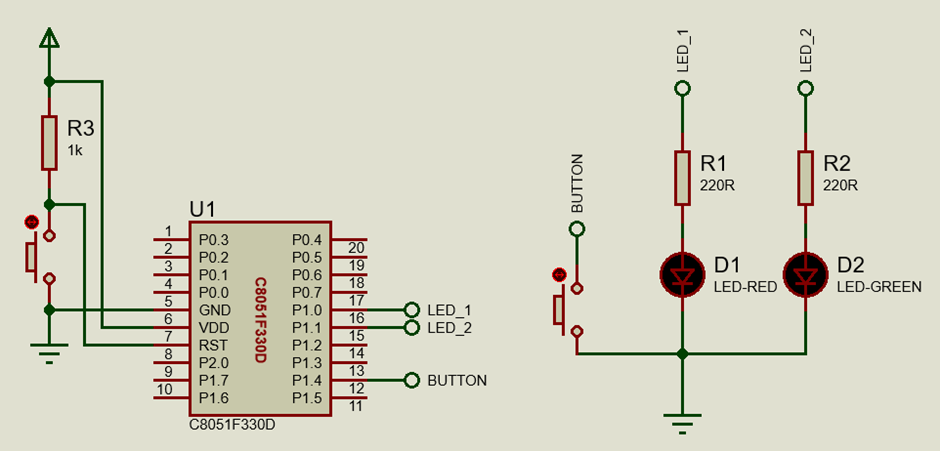
Schematic
Explanation
To demonstrate both the clock system and the GPIOs, I used a simple LED blinking example.
Two LEDs connected with P1.0 and P1.1 blink alternatively like a police light. These pins are set as push-pull outputs.
A push button connected with P1.4 is also set as an open-drain input. An open-drain input is not purely open from VDD as there is a weak internal pullup. The purpose of this button is to change the clock frequency by altering the clock divider.
 void Port_IO_Init(void)
 {
     // P0.0  -  Unassigned,  Open-Drain, Digital
     // P0.1  -  Unassigned,  Open-Drain, Digital
     // P0.2  -  Unassigned,  Open-Drain, Digital
     // P0.3  -  Unassigned,  Open-Drain, Digital
     // P0.4  -  Unassigned,  Open-Drain, Digital
     // P0.5  -  Unassigned,  Open-Drain, Digital
     // P0.6  -  Unassigned,  Open-Drain, Digital
     // P0.7  -  Unassigned,  Open-Drain, Digital

     // P1.0  -  Skipped,     Push-Pull,  Digital
     // P1.1  -  Skipped,     Push-Pull,  Digital
     // P1.2  -  Unassigned,  Open-Drain, Digital
     // P1.3  -  Unassigned,  Open-Drain, Digital
     // P1.4  -  Skipped,     Open-Drain, Digital
     // P1.5  -  Unassigned,  Open-Drain, Digital
     // P1.6  -  Unassigned,  Open-Drain, Digital
     // P1.7  -  Unassigned,  Open-Drain, Digital

     P1MDOUT = 0x03;
     P1SKIP = 0x13;
     XBR1 = 0x40;
 }
By default, the internal high-frequency oscillator is selected as the system clock source. This source is reasonably accurate for typical applications. Inside the code, the oscillator divider is altered to change the system clock frequency.
 void main(void)
 {
     unsigned char i = 0;

     Init_Device();

     P1_0_bit = 1;
     P1_1_bit = 0;

     while(1)
     {
        if(P1_4_bit == 0)
        {
            delay_ms(100);
            i++;
        }

        switch(i)
        {
            case 0:
            {
                OSCICN = 0x83;
                break;
            }
            case 1:
            {
                OSCICN = 0x82;
                break;
            }
            case 2:
            {
                OSCICN = 0x81;
                break;
            }
            case 3:
            {
                OSCICN = 0x80;
                break;
            }
            default:
            {
                i = 0;
                break;
            }
        }

        P1_0_bit ^= 1;
        P1_1_bit ^= 1;
        delay_ms(100);
     };
 }
Since the software delay amount is fixed, changing the system clock frequency alters the blink rate.
A word of caution that I would like to share at this point that is, the internal watchdog timer (WDT) is started but default and so we need to stop it before doing anything else. If this is not done then our code would seemingly not work at all as the WDT would repeatedly overflow and reset the microcontroller. In C8051s, the WDT is a part of the PCA module and so the PCA module needs to be configured as follows.
 void PCA_Init(void)
 {
     PCA0MD &= ~0x40;
     PCA0MD = 0x00;
 }
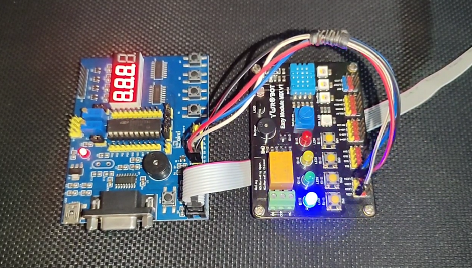
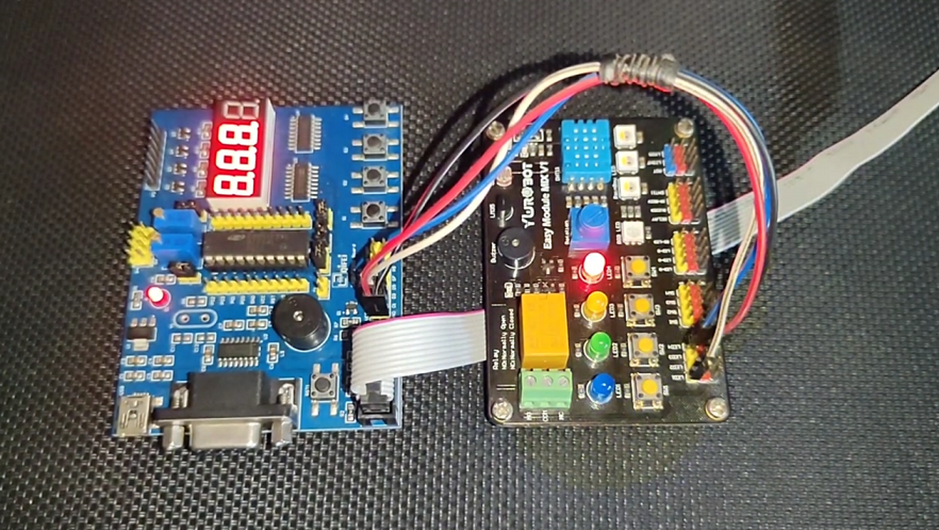
Demo
|
|
Thanks for the feedback….